This thread has been locked.

If you have a related question, please click the "Ask a related question" button in the top right corner. The newly created question will be automatically linked to this question.

SN6501: Rise - Fall Time & Frequency FOR D1/D2 is not as per expected values from datasheet

Part Number: SN6501

I am using SN6501DBVR for Generating Isolated 5V Supply. But while Carrying Out Internal Testing, found Out that the Rise-Fall Times are higher  & Frequency is lesser than expected for D1/D2.

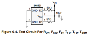
VCC = 3.3V. My circuit is similar to that mentioned in datasheet, with only change being that of 10uF instead of 4.7uF near TP1 (Input of LDO). I have attached snap of circuitt schematic from your datasheet for reference.


Sr. No Signal Parameter Expected - Min  Expected - Typical  Expected - Max  Observed
1 D1/D2 Rise Time (nS) - 70 - 120
2 Fall Time (nS) - 110 - 130
3 Frequency (KHz) 250 360 550 220.4

Please help me on this !!!!

  • Hello Srikrishna,

    Thank you for reaching out. The circuit below is a simplified setup used to evaluate device performance and operation. It was used to measure the values in 5.6 Switching Characteristics that you listed previously. The reason a test circuit is used is to remove the effect of the transformer from the measurement, which will affect rise and fall times.

    The switching frequency of 220.4kHz is interesting though. Please provide a screen capture of this happening for us to evaluate. 

    Best,
    Andrew

  • Kindly Find above attached snap, which illustrates D1-D2 Frequency.

  • Hello Srikrishna, 

    Thank you for providing the screen capture. To debug further, please see below.

    1. Can you please test the circuit as shown in Figure 6-4 above? This will eliminate any system elements and help us verify the device.
    2. Are you seeing this behavior on any other devices? Or is this the only sample being tested? 

    Best,
    Andrew

  • I have observed this Behavior on One Sample Which I have tested so far. Will test more samples and verify it's behavior. Will even Test the circuit as per Figure 6-4.

  • Okay thank you for the updates. I will wait for the results. 

    Best,
    Andrew