This thread has been locked.

If you have a related question, please click the "Ask a related question" button in the top right corner. The newly created question will be automatically linked to this question.

ISO6762: Isolated ADC's SPI tested for communication with errors at ESD-HCP-8kV

Part Number: ISO6762
Other Parts Discussed in Thread: STRIKE

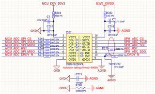
Hello, I am using ISO6762 to isolate the SPI communication bus of my ADC device, and when testing the HCP for ESD, I found that it has an effect on the communication, it will incorrectly output the DRDY signal of the ADC, and the value of the ADC conversion received by the SPI will be incorrect, which doesn't exclude that the DRDY is being triggered in advance to read the wrong data. When I remove the isolation and connect the GND of the isolated signal with a wire, the test can pass; when I put back the isolator and keep the isolation GND shorted, the test will be wrong; when I remove the isolation GND, the test error will become very frequent, I tried to replace the isolator IS3762 from other vendors, and it is OK to pass in the same PCBA, so I suspect that there may be a problem with the ISO6762. I hope to get your reply and support, thanks!

  • Hello Yivi,

    Thank you for reaching out. can you please share input and output waveforms of the ISO6762 during the test? Please share a schematic if possible since this is more of a system level test.

    Best,
    Andrew

  • Hi, I have captured some waveforms, please help me evaluate them. I don't see a problem from the waveforms, they are almost simultaneous or my test method might be wrong. The test was done using a 100Mhz bandwidth oscilloscope.
    There is some sensitive information in the schematic, is it possible to send it via e-mail?

    Thanks for your help, looking forward to a reply, good luck!

    Input and output waveforms of ISO6762 and IS3762.pdf

  • Hi Yivi,

    Andrew is currently looking into it. Please allow him to come back to you with inputs, thanks.


    Regards,
    Koteshwar Rao

  • Hello Yivi, 

    I have sent a friend request and a direct message on E2E you can share your schematic via private message. 

    I have reviewed your input and output waveforms and I do not see any obvious issue. 

    • The failure conditions for the test is the MCU receiving a false communication on PIN 7, correct? 
      • The report mentioned a filter capacitor was removed, which capacitor was this? The filter capacitor on the supply pin is intended to limit ringing from possible supply transients and is needed for operation.  
    • Where is the 8kV ESD strike applied and how is it connected to the ISO6762?

    Best,
    Andrew

  • thanks for you reply.

    1. Yes, the MCU receives the pulse signal suspected to be present on the ISO6762, this signal is used to alert the MCU that the data conversion of the ADC is complete, it is very important, if triggered incorrectly it could result in an SPI interrupt or an error in reading the converted value.

    2.Some RC filters are reserved on the isolation channel of the isolator, and for testing we removed the filter's C,a 22pF capacitor; the capacitance of the isolator's power supply section is retained, and it contains a 0.1uF and 10uF ceramic capacitor filter.

    3.8kV ESD is applied to the HCP metal coupling plate, which affects the isolator or my system design by means of spatial coupling.

    I will send you the system block diagram, schematic, and test description documents in a private message later, thank you!

  • In our testing, we found that adding a small piece of copper foil underneath or on the back of the isolator improved the HCP, which indicates that there may be interference inside the isolator, or that the copper foil forms a capacitor with the ground on either side.

    The soldered end is the ground of the ADC, which is the N of the three-phase power supply.

    Copper foil without any links.

  • Hello Yivi, 

    The schematic looks good. I suspect that the foil is acting as a Y-capacitor that is close to the IC, which is providing some additional ESD/EMI protection. It may be necessary to include an additional Y-capacitor close to the isolator's GND pins in the application. 

    I will continue to review the information in more detail. 

    Best,
    Andrew

  • Yes, I've tried connecting a Y capacitor across next to the isolator, but it didn't work.

  • Hi Yivi,

    Could you please let us know what value of Y-capacitor did you use and where was is it located?
    It is necessary to keep the Y-cap as close as possible to isolator ground pins for it to be effective in suppressing noise. Connecting between pins 8 and 9 would be ideal. Thanks.


    Regards,
    Koteshwar Rao

  • I've tried 1000pF and 2200pf, which are spanned near ground closer to the 1-16pin,Jumpered at 8-9Pin I didn't test, but the results should be the same.

    Best,

    Yivi

  • Hello Yivi,

    We will review all of the information again and get back to you. Does adding the metal foil completely solve the issue? 

  • Adding copper foil improves it a lot, but doesn't solve it completely, thanks

  • Hi Yivi,

    Thank you for sharing all the requested information so far.

    I have reviewed the waveform again and it looks like the <20ns glitch produced at the output OUTF is an external coupling. This is not a glitch generated by device output OUTF or passed from input INF to output OUTF as the device is not capable of passing such pulses to the output. The pulse/glitch seems to have coupled to the output pin  through external parasitics.

    The best way to address this is to add an RC filter at the output OUTF of ISO6762 pin. I see the schematic has RC filter at the input pin INF but not at the output. Please add a 22pF or 33pF capacitor at the output pin OUTF after the 100Ω resistor R273 such that the R and C form a low pass filter and filter out the glitch. Since DRDY is a 100ns pulse, it shouldn't be affected much. If the DRDY signal doesn't look satisfactory then you can increase / decrease the output filter capacitor to the point where DRDY is clean and the glitch is filtered out.

    Please consider performing this test and let us know the results. Thanks.


    Regards,
    Koteshwar Rao

  • Hi Koteshwar,

    I've tried 22pF and TVS,But it doesn't improve the test.

    Regards,
    Yivi

  • Hi Yivi,

    Could you please confirm if the 22pF was connected at the OUTF (pin 7) after resistor R273?

    It is also important this capacitor has a good connection to GND1 (pin8). Since there is no capacitor footprint on board, this has to be soldered externally. Could you please share a photograph of the PCB with this capacitor soldered?

    Could you please also share INF and OUTF waveform after the RC filter?


    Regards,
    Koteshwar Rao

  • Hi Koteshwar

    I'm very sorry for being away for so long, during this time I have adjusted the isolation scheme to solve the BER problem for critical communications by means of no isolation, the fault tolerant SPI channel is based on the 6762 isolation used, and there are still BER's when testing the HCP, but adjusting the isolation scheme makes the BER requirement for the SPI lower, so it is feasible, and this issue may require me to find the time to test it once I have completed this project.

  • Hello,

    Please note that today is a holiday in the US, we will review your inquiry and respond tomorrow.

    Thank you for your patience.

    Best,

    Michael

  • Hi Yivi, 

    Thank you for your reply and thanks for the update.

    I understand that you have re-designed without using the isolator device in the PCB and that you will test it again in the future. If you have any more questions, we are more than happy to help.

    As Koteshwar mentioned, the requested information may help us understand the customer's issue better and provide you with some more information as well.

    Regards,
    Aaditya Vittal

  • Thank you for your help and let's follow up.