Part Number: SN74AVC4T245
Other Parts Discussed in Thread: SN74AXC4T245, SN74AXC8T245
Hello,
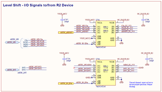
I'm trying to use two SN74AVC4T245 chips as simple level translators between a MCU (1V8, always on) and a peripheral (3V3 when on but usually powered down). The arangement is shown in attached picture. 4 I/O signals going out from the MCU and 3 coming back in the opposite direction.
I'm finding that when the 3V3 supply on port B is powered down, the lower of the two devices shown is causing a high sleep current to be drawn, presumably from the 1V8 supply (VSUP_MCU). In this state, pins 1 and 16 of both devices are set high by an MCU I/O line, to disable the outputs.
On the upper device (which seems to have no problems) the 4 inputs on the left are driven low by the MCU. The 3 signals on the lower device go to MCU inputs which are disabled, so effectively all signals on the A port see Hi-Z. The B port is powered down and close to 0V, with the B inputs also close to 0V.
Having found this issue I've looked again at the datasheet and note this on the front page:
"The input circuitry on both A and B ports is always active and must have a logic HIGH or LOW to prevent excess ICC and ICCZ."
I guess this means I need some kind of pull down to prevent them floating, so questions are:
1 - should I have pull-downs on the B inputs, even though this side is powered down? If not essential I'd rather not as this board is extremely tight.
2 - for the unused signal on 1A2/1B2, is it safe to connect 1A2 direct to ground given that this is an output, or is it necessary to add something like 10k to ground on both sides? Again, I'd rather not as I'm very short of space.
3 - when B port is powered down and output enable is high to disable outputs, is it possible to minimise current on the other port if the signals on the A port are properly pulled down?
Thanks,
Gordon.