


Hi Team,
We are doing 9U board design, in our design Artix7 family FPGA used. FPGA to Back plan we have VME interface, that interface trace length should be around 12inch.
1) 96 pin connector to level translator 2 inch, Trace with 5.1 @ 50 ohm impedance.
2) Level translator to FPGA 10 inch trace length, Trace with 5.1 @ 50 ohm impedance.
Level translator part number: SN74LVC16T245 (16-Bit), SN74LXC8T245QPWRQ1 (8-Bit).
We are did SI simulation for VME interface. Result are given in below.
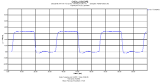
1) FPGA (LVCMOS_3V3_8mA) as driver LVT (3V3) as receiver at the time signal (transmission) quality is good (Overshoot and undershoot are with in range).
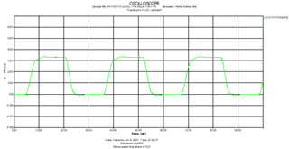
2) LVT (3V3) as driver FPGA as receiver at the time signal quality is bad. ( we are getting Overshoot and undershoot are with in range)
The issues are listed.
1) LVT to FPGA signals transmission line required series termination. it is really required or we have any other approach?
2) VME interface Data bus is BI-Dir bus. this signals some time LVT as driver some time FPGA as driver, in this case where we can mount series termination? or we have any other approach?
3) For Data bus How we can control Overshoot and undershoot with out series termination?
Our trace length is 10 inch (max) LVT to FPGA. For this trace length who we can achieve with good signal quality, please recommend any design approach.
Our SI simulation report is given below. please refer.
Case 1: Artix7 to level translator
FPGA part number: XC7A200T-1FBG676C
FPGA Buffer model: LVCMOS33_F_8_HR
Level translator part number: SN74LXC8T245QPWR
Buffer model: input_3.3V
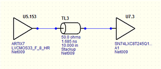
Trace length: 10 inches
Trace width: 5 mils
Frequency: 32 MHz
- Waveforms:
Case 3: Level translator to Artix-7
FPGA part number: XC7A200T-1FBG676C
FPGA Buffer model: LVCMOS33_F_8_HR
Level translator part number: SN74LXC8T245QPWR
Buffer model: input_3.3V
Schematic:
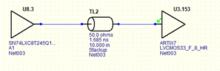
Trace length: 10 inches;
Trace width: 5 mils
Frequency: 32 MHz
Waveforms:

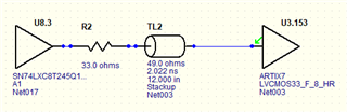
Case 4: With 33 ohms series termination:
Level translator to Artix-7
FPGA part number: XC7A200T-1FBG676C
FPGA Buffer model: LVCMOS33_F_8_HR
Level translator part number: SN74LXC8T245QPWR
Buffer model: input_3.3V
Schematic:
Waveform:
Regards,
Sivakumar R
