This thread has been locked.

If you have a related question, please click the "Ask a related question" button in the top right corner. The newly created question will be automatically linked to this question.

LSF0108: Rising edge during the Translating UP

Part Number: LSF0108
Other Parts Discussed in Thread: TINA-TI, SN74AXC1T45, , SN74AVC4T245

Hello,

While I look into how LSF device works, I ran into an e2e thread (please find the original thread) and I have a question.

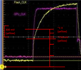
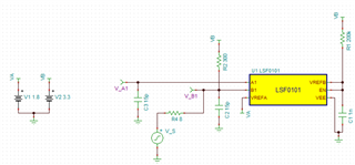
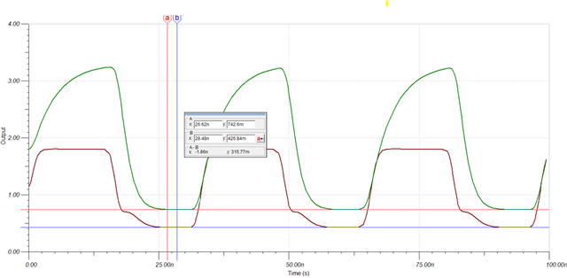
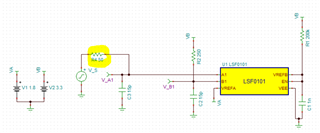
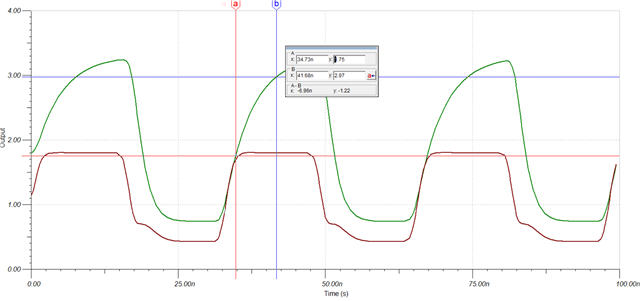
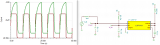
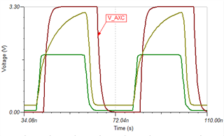
In the original thread, there is a waveform as below - A side (purple) input to B side (yellow) output.

I do not understand why the yellow waveform do not track the purple waveform on its rising edge.

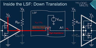
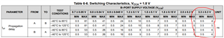
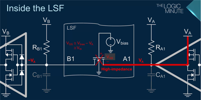
To my knowledge so far : For Translating UP, B1 node voltage would immediately track the A1 node upto ~VA, and then rises following RC (2*RB1*CB1). 

Could you help me to find the reason of discrepency between the waveform from the original e2e thread and my undertanding?

Thanks,

  • It looks like you've found the Logic Minute videos on this topic, and are on the correct video (Up Translation)

    I think your understanding is good from your explanation - but there is some nuance I can help to explain.

    First, the scale of the two waveforms is not the same, which makes it more difficult to compare waveforms directly:

    Looking only at the output waveform, we can see clearly where the RC circuit takes over:

    From the 0V reference, the output starts following an RC curve at about 750 mV.

    There are two additional factors causing issues here. 

    (1) The device is being operated at a very low voltage bias 1.05V -- this means that the channel will have increased resistance and will turn off easier than at higher voltages -- ie the RC will take over at a lower voltage.

    (2) This difference in supplies is less than the recommended 0.8V, which can result in some reduction in the voltage at which the output switches and can cause variation in the clamp voltage due to incorrect bias.

    I ran my simulation again and focused on the rising edge for this up-translation:

    The simulation also predicts that the RC takes over at approximately 0.7V under these conditions.

    My simulation file:

    LSF0101_example_timing_rising_edge.TSC

  • Emrys,

    Thank you for your detailed explanation. I have additional question on Translating Down. I tried to run the simulation from 3.3V to 1.8V, expecting that the rising edge of the A side (1.8V) would directly track the rising edge of the B side (3.3V), because the pass FET would be on its turn-on status until A1 node rises up to VA. It's being operated at a high voltage bias 3.3V. 

    But what I observe in the simulation is as below. It looks the pass FET turned off earlier than I expected, thereby rising edge looks like RC charging even before A side reaches at 1.8V. Why the pass FET turned off so early?

  • Emrys,

    I also have a question on Translating Up. There appears VOL due to the pull-up resistor on the B side.

    For 30.72MHz signal transmission, I choose 300ohm pull-up resistor on the B side. Fco = 1/2piRC = 1/(2*pi*300*15p) = 35.36MHz

    VOL appears 742.6mV. It's so high. (I set R4 into 50ohm in order to model the driver with Zo=50ohm, which noted in the datasheet page 9)

    I'd like to ask for your advice :

    1. Would I actually see this high level of VOL on the bench? If not, how do I modify the tina circuit to properly model the driver/receiver on the A/B side each.

    2. When it comes to my setting on Zo=50ohm, did I model it correctly?

    3. Datasheet says " The LSF family of devices supports up to 100- MHz up translation and greater than 100-MHz down translation at ≤ 30pF cap load". So I guess 15pF of CL in my simulation is not that heavy. But the simulation result is quite pessimistic because its SI looks not good for me. The rising edge of 3.3V output is too slow. 50%VOUT to 90%VOUT takes 6.96ns in 30.72MHz clock signal transmission. So I'm worried the situation that the receiver cannot pick up its rising edge on time. Could you advise on the discrepency between datasheet and the tina simulation result?

  • 1. Would I actually see this high level of VOL on the bench? If not, how do I modify the tina circuit to properly model the driver/receiver on the A/B side each.

    Yes, that is very likely. With a 50 ohm driver and 250 ohm pull-up resistor you will get up to 11 mA of current through the channel. With a 30 ohm channel resistance, this would produce 30 * 0.011 = 330mV of voltage drop across the device, which is approximately what the simulation is showing.

    Your driver will need to be _much_ stronger than 50 ohms to have a clean 30.72 MHz signal. You can see that your input signal is already 470mV off of ground before going through the LSF, which is going to add to your VOL level. Changing to an 8 ohm or less driver will improve that significantly

    2. When it comes to my setting on Zo=50ohm, did I model it correctly?

    Zo is a characteristic impedance - it is not a resistance. Additionally, it's not requirement for a logic system to use 50 ohm matched lines -- these are best implemented when the driver, line, and load are all the same impedance. I have an FAQ that goes into some details on the effects of using transmission lines with logic devices here: (+) [FAQ] What happens when I connect a logic device's output to a 50 ohm transmission line? - Logic forum - Logic - TI E2E support forums

    Tina-TI isn't designed to show signal integrity over transmission lines - this is best reserved for IBIS model simulators like ADS and Hyperlynx.  

    I also see that you haven't changed the parasitic capacitances to match your system. This is critical for you to get any idea of actual operation. If you have 50 ohm transmission lines, they will have significant capacitance -- you may want to use an online calculator to determine the capacitance based on your board geometry/configuration.

    3. Datasheet says " The LSF family of devices supports up to 100- MHz up translation and greater than 100-MHz down translation at ≤ 30pF cap load". So I guess 15pF of CL in my simulation is not that heavy. But the simulation result is quite pessimistic because its SI looks not good for me. The rising edge of 3.3V output is too slow. 50%VOUT to 90%VOUT takes 6.96ns in 30.72MHz clock signal transmission. So I'm worried the situation that the receiver cannot pick up its rising edge on time. Could you advise on the discrepency between datasheet and the tina simulation result?

    I agree that 100 MHz is really pushing the limits of the LSF translator, but that's why the datasheet says "up to" instead of "excellent signal integrity at." I would not generally recommend this device for such a fast signal, but it's possible to make it work under good conditions.

    Above is the same simulation, with a very strong driver (1 ohm) and 15 pF loading operating at 100 MHz.

    To be clear - if your system needs fixed-direction voltage translation, I would always go with a different solution. For example, SN74AXC1T45 will produce much cleaner and better signals for 1.8V to 3.3V translation.

  • Emrys,

    Thank you for all your comments. It helps a lot. 

    For example, SN74AXC1T45 will produce much cleaner and better signals for 1.8V to 3.3V translation.

    Customer is deciding either LSF0108 or SN74AVC4T245. They're thinking LSF is a better option for 30.72MHz and 25MHz clock level converting application because LSF has smaller delay than SN74AVC4T245. But it looks LSF0108 may cause a problem in the application due to its slow rising edge. 

    I want to double-check the delay spec. Generally, LSF family has smaller delay than SN74AVC/AXC family. Is it correct?

    <SN74AXC1T45 datasheet>

    In addition, could you also kindly check my question regarding the DOWN translating? I have two 'Reply' above, one is for DOWN translating and the other is UP translating. Thank you again for your comment on the UP translating.

  • Thank you for your detailed explanation. I have additional question on Translating Down. I tried to run the simulation from 3.3V to 1.8V, expecting that the rising edge of the A side (1.8V) would directly track the rising edge of the B side (3.3V), because the pass FET would be on its turn-on status until A1 node rises up to VA. It's being operated at a high voltage bias 3.3V. 

    But what I observe in the simulation is as below. It looks the pass FET turned off earlier than I expected, thereby rising edge looks like RC charging even before A side reaches at 1.8V. Why the pass FET turned off so early?

    MOSFETs are analog devices - they don't turn on and off perfectly at some precise voltage - they gradually change states. My explanation in the video is simplified for brevity - I would probably need a full semester course to explain this in detail (many engineering schools teach MOSFET operation in the first or second year as an independent course).

    Since the channel voltage is small (V_DS), then the device will be operating in the ohmic (or linear, non-saturation) region of operation, which means the current is going to be (approximately) linearly related to the voltage across it, acting like a resistor.

    Decreasing V_GS, the control voltage, the device will have increased resistance.

    Additionally, as the input/output voltages increase, V_GS decreases while V_DS increases (due to increased resistance) and eventually the device will go into the saturation region (V_DS > V_GS - V_T), at which point the device acts more like a current source than a resistor.

    This is all just to say that the simulation is taking all of these changes into account and is providing you with a relatively accurate picture of what the device is expected to do. It's not perfect -- no simulation is -- thus why I recommend building the circuit instead.

  • I want to double-check the delay spec. Generally, LSF family has smaller delay than SN74AVC/AXC family. Is it correct?

    <SN74AXC1T45 datasheet>

    Yes, buffered devices have delay, and your screenshot fromt the datasheet is accurate.  However, an AXC translator will be actively driving the output, which will mean the signal integrity will be vastly better than an LSF type translator.

    I ran a quick simulation to show the expected comparison above. You can see that the LSF does have less delay - depending on where exactly you measure it. At 50%, 1.65V, the LSF only has 2ns of delay (measuring from the 50% mark of the input signal, 900mV).

    The AXC device has a delay of 2.86ns, but has much better signal integrity.

  • I should also note that the LSF model being used here is very basic - only showing the lowest level of MOSFET model that can be released, so the accuracy will be impacted. The best answer is to use the actual device in a prototype circuit.

  • Emrys,

    All your comments help a lot. Thanks a lot.