


Dear Sir
1) it works very well when I wrote any data into BANK0 and then erase it. but it was failed to do same thing for BANK1 to BANK7, after I wrote some data into BANK1 to BANK7, I read memory cells, they are still 0xFF,
What are the differences between the BANK0 and other BANKs?
2) the application note(slva550a) said:
"Writing to the arrays is not significantly impacted from a protocol standpoint. If a bank/pump is sleeping and a program command is initiated, the SM28VLT will automatically begin the wake up process and complete programming without further need for host to be involved (page6)"
Can it enter sleep mode again automatically after the program process ends?
3) I wrote the different values into the BAC1 register for different BANKs, When I read it back, all the BAC1 registers have the same value and the value is decided by the last one I wrote. it the same thing for the BAC2 register. what are the reason?
4) For the MAC2 register. the application note (slva550a) said: " These bits must be left at 000 (Page 4)" ,but in the Psuedo Code of the note, the last line is "1D_000F001_00C1 // set pump pwr dn fallback mode to standby".
according this code, the MAC1.BANK is 001, not 000, I think only one is right, could you tell me which one correct? someone asked same question 6 years ago, but I don't see the answer
5)
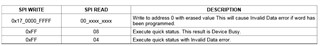
how to understand " Write to address 0 with erased value This will cause Invalid Data error if word has
been programmed."? is the address 0 cell special?
Clark


