Other Parts Discussed in Thread: SN74AHC573, SN74AHC541, SN74LV541A, SN74LVC541A
Hi Team,
Please see the issue description as below. Thanks.
Roy
This thread has been locked.
If you have a related question, please click the "Ask a related question" button in the top right corner. The newly created question will be automatically linked to this question.
Hi Team,
Please see the issue description as below. Thanks.
Roy
These signals violate the setup and hold times specified in section 7.6 of the datasheet.
What is the purpose of using a flip-flop in this circuit? Why are you mentioning the '245 transceiver? It's possible that that device, or a transparent latch like the SN74AHC573 might work better.
Hi Ladisch,
We want to check tsu and th with you.
For tsu, does it mean that we need input the data at least 4ns before clk posedge?
For th,the data status need to hold at least 2ns and the time duration need to smaller than clk high time?
Roy
Hi Ladisch,
Below is our purpose. We use the chip to be the level shifter. After the chip, we want to transfer signal from 3V-5.5V to 3.3V. We used CLKOUTIN as DCLK and DEIN as example.
Did you mean the SN74AHC573 may be a better solution for us?
Roy
Hi Lasdisch,
We need all of our signals output waveform should be synchronized. (Meanwhile, signal level should shift to 0-3.3V. So we used three D flip-flop and same CLK to trigger them.
Regards,
Roy
Hi Ladisch,
For schematic, I showed in the top. All of SN74AHC574 share the same CLK(TICLK) because we need all of our outputs changed at the same time. That's our purpose. And for input signal, the high level range will be 3V~5.5V. We also need to use D-flip flop to shift all of high level to 3.3V.
May SN74AHC573 be a better solution for us?
Regards,
Roy
Hi Ladisch,
Please see below. Honestly, I'm not sure why we can't get the expected output signal. Can you let me know if there is any appropriate solution(SN74AHC573?) that fit our request. If SN74AHC574 can fit our request, can you kindly let me know the reason that we can't get expected results? How to solve it? Many thanks.

RRegards,
RRoy
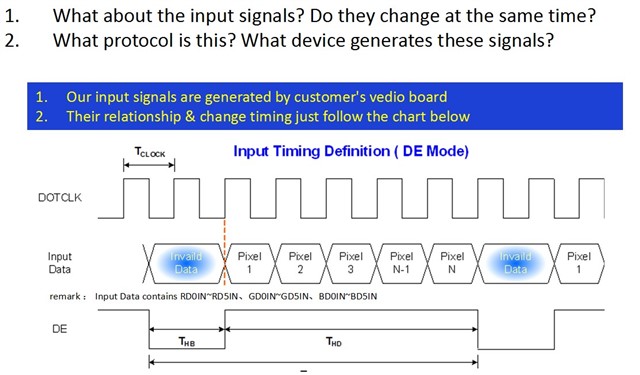
In this protocol, the transmitting device changes the data at the rising edge of the clock, while the receiving device samples the data at the falling edge of the clock.
If you wanted to handle this protocol with flip-flops, you would be receiving and transmitting, so you would need to delay all signals by a half clock cycle. This would be possible, with an inverter on the clock signal.
But all that is not necessary. The input signals already are synchronized, so you need only simple buffers. Use 3× SN74AHC541 or SN74LVC541A.
Hi Ladisch,
I am the EE R&D from AU Optronic .
As Roy's reply, our application requirement is only to change the amplitude of the input signal,without changing the relative relationship between them.
I guess your SN74AHC573 may achieve this function does it ?
So please give me some advice of device choosen.
Many Thanks!
When LE=H , output Q wlways follow input D
INPUTS OUTPUT
/OE LE D Q
L H H H
L H L L
L L X Q0
H X X Z
Thank you for your quick response.
I will evaluate this device what you suggested.
Thank you!
The 573 can indeed be used as a buffer. But it would be simpler to use a buffer as a buffer.