This thread has been locked.

If you have a related question, please click the "Ask a related question" button in the top right corner. The newly created question will be automatically linked to this question.

TXS0102: TXS0102

Part Number: TXS0102

Hello there!!

We think we are having problems with the TXS0102DCTR level converter.

We connect our system, through a TXS0102DCTR, to a BG96 NBIOT modem, as it´s specified in datasheet, but at communication it is impossible to send / receive messages through the uart.

Previoues information: 

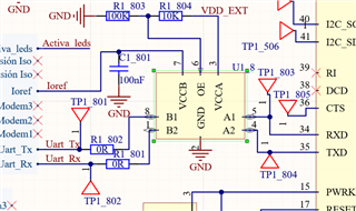
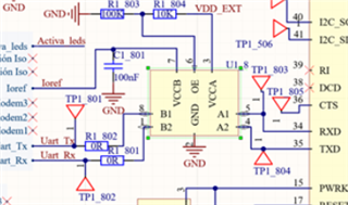
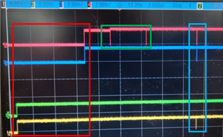
TX (Master) -> TP1_801 (Yellow line) -> Voltage-Level Translator -> TP1_803 (Blue line) -> RX (Modem)
RX (Master) <- TP1_802 (Green line) <- Voltage-Level Translator <- TP1_804 (Pink line) <- TX (Modem)

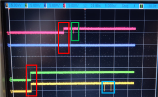
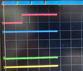
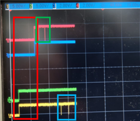
As you could see on the image:

- The modem RX line (line blue) remains inactive.

- The messages sent by the modem, although the line seems active, are not transferred through the level converter.

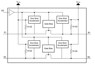
Despite voltage level translator has internal pull-up resitor, these dont appear to be enougt to maintain an adequate level

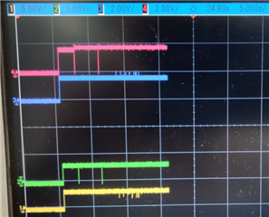
We have tried to include two pull-up resistors (10kohm) on RX and TX lines (modem side), which helps to keep the level of RX signal at a correct value. 
But communication doesn't work although.


We have tried to change the IC for another (removing the pull-up resistors too). 
The RX value doesn´t take a correct level, but at least System->Modem communication works (cause modem understand the message and try to ansswer), but Modem->System lines dont work properly

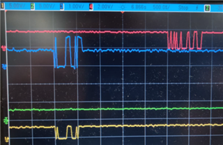
We have tried to include the pull-up resistors again together with the new IC, but the case is similar to the previous one, except that the RX line have a correct level.

We do not know what is happening. Any help is welcome
  • The third screenshot looks strange. Was channel 3 in AC mode? This looks as if two devices are trying to pull this line up and down.

    The TXS is a passive switch, so maybe the modem's RX pin sometimes works as an output? Or are there pull-down resistors anywhere?

  • Hello, first of all thank you for answering.

    No, channel 3 was settup as DC mode. 

    In the case shown in image 3, there was no pullup or pulldown resistor on the RX line that goes from modem to converter and there is only the modem controlling that line (same as the first schematics image)

    In my opinion, it´s like voltage converter internal pull-up resitor can´t active RX line to a valid value. 

    In other test, we add some external pull-up resistors to these line (RX and TX). Second screemshot. And RX line then get VDD_EXT (1,8V) 

    The TXS is a passive switch, so maybe the modem's RX pin sometimes works as an output?

    We cant check it, but following BG95 datasheet it appers complicated.

  • If two chips behave differently, then it's likely that at least one of them is damaged.

    Anyway, can you capture the waveform with a much higher sample rate? I suspect that the lines are oscillating. (Are there long traces/cables in the circuit?)

  • Maybe this new test confirm some doubt about it.

    We have disconnect TX and RX line from master (left floating), so voltage converter has power in both sides (VccA and VccB) but only TX and RX connected to modem, in modem side.

    After modem activation (and VDD_EXT activation that powers the converter) we see that only the TX signal on the modem side is activated.

    This behavior is very different if we compare it with the other boards that do work propoerly, as you could see in the following image:

    Anyway, can you capture the waveform with a much higher sample rate?

    Please, tell what do you want to see better and I repeat test and take better screemshoot for you?

    Are there long traces/cables in the circuit?
    Since we are testing the circuit, the boards are connected through the "typical arduino cables"


    f two chips behave differently, then it's likely that at least one of them is damaged.

    In this order we have manufactured 5 boards. Isn't it a little weird that all ICs of 5 boards are damaged?

    We are going to talk to our manufacturer anyway.

     
  • Hey Adrian,

    What is the state of the OE pin during these tests? These waveforms don't really make sense even if there was some damage to the device. This device is passive, so when nothing is driving the I/O, they should remain High (there is no circuitry that drives Low in the translator). I would isolate the translator completely and measure the I/O to make sure this behavior happens, I would also have one scope channel on the OE to fully confirm its at the right state. If this doesn't happen then its possible the device is damaged.

  • Hello Dylan!

    We work in 3 phases: 

    1. We power-up master and conversor VccB with 3.3V. EO stay deactivate (0v)

    2. We power-up modem, but we dont activate it, so VDD_EXT keep 0v and EO too.

    3. We activate modem so VDD_EXT become 1.8V; VccA get 1.8v and EO get 1.637v

    There is no noise, or glitches, or bounds at EO pin.

    All screemshots before were taken during the third phase, but logically the same process was followed, and we check voltage over differents stages. Additionally, we have compared level of the voltage converter pins for a new IC and the old one, and we have not obtained differences.

  • Hey Adrian,

    Thanks for the info, were you able to isolate the device I/O and test in phase 3? 

  • Sorry, I skip your question before.

    We cant fully isolate the IC cause modem RX and TX lines go directly to that. We can perfectly disconnect master lines although; and we can sniff signal using testpoint (as you could see on schematics), but a fully isolation appers imposible without desoldering elements

  • Hey Adrian,

    To verify if its the device is damaged or if the problem lies with the interfacing devices, this will be the best way.