Part Number: CD4047B-MIL
Dear Team,
Could you help to check the schematic as below?
it's a inverter application.
Spec:
Vin 12V Vout :54V ac 60W

Many Thanks,
Jimmy
This thread has been locked.
If you have a related question, please click the "Ask a related question" button in the top right corner. The newly created question will be automatically linked to this question.
Part Number: CD4047B-MIL
Dear Team,
Could you help to check the schematic as below?
it's a inverter application.
Spec:
Vin 12V Vout :54V ac 60W

Many Thanks,
Jimmy
Hey Jimmy,
I would recommend against connecting a potentiometer (VR1) directly between pins 2 and 3. This could result in applied resistance below the datasheet recommended range, which could cause damage to the device.
I would recommend to add a series 10kohm resistor between pin 2 of the CD4047 and pin 2 of the 100k potentiometer to ensure that the resistance is never less than 10k between pins 2 and 3.
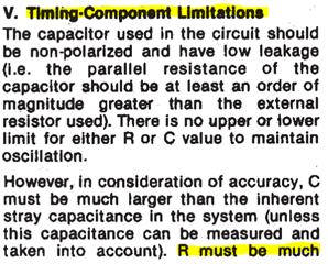
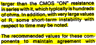
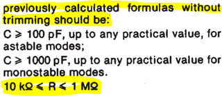
-
As the circuit is shown, we would expect this configuration to produce an output signal down to ~5.1 Hz with VR1 = 100kohm (97 ms pulse width) at Q and Q\.
Adding a 10kohm resistor would decrease the minimum value to ~4.7 Hz.
In either case, the maximum frequency is ~51.7 Hz, assuming the recommended 10kohm minimum R value is not violated.
Hi Emrys,
We appreciated your great support!
Customer have modified the schematic. Could you help to check it? Thanks!
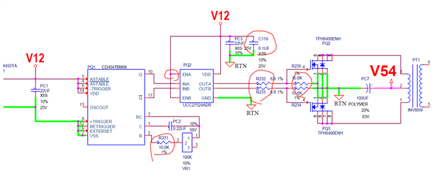
Many Thanks,
Jimmy
Hi Emrys,
We appreciated your great support!
We used CD4047BM96 to do the oscillator, so the CD4047BM96 has some deadtime, right?
Many Thanks,
Jimmy
Hi Jimmy,
No, the CD4047 as configured is just an oscillator -- the outputs will switch at the given frequency, with perhaps a few nanoseconds of difference between the two output signals.
There is no dead time circuitry in the device.
Hi Emrys,
Thanks for your great support!
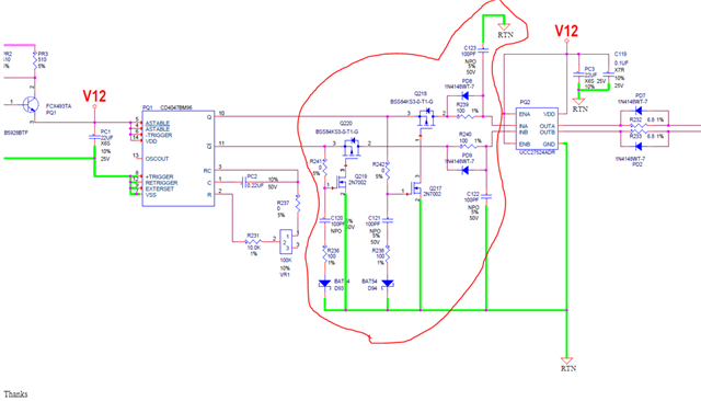
Our customer add deadtime circuit, could you help to review it? Thanks!
Many Thanks,
Jimmy
Hi Jimmy,
I don't see any problem with connecting that circuit to the CD4047. The added series resistance on each capacitor should prevent any excessive current.
I'm not certain of how the circuit is intended to function -- it looks to me like Q220 and Q218 will never be turned off:
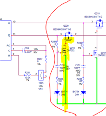
There's no path for charging the gate, so it will either be pulled low or left floating, which may result in some unexpected behavior.
Hi Emrys,
We appreciated your great support always!
Could you explain why Q220 and Q218 will never be turned off.
If customer want to add delay circuit, could you guide us how to do that is right? if you can, please draw on the schematic. Thanks!
Thanks a lot!
Jimmy
Hi Jimmy,
To turn off a pFET you have to charge the gate so that VSG < |VTP| -- there is no circuit here that can charge the gate up to 12V from what I can see. There is only a discharge path through Q219 or Q217.
Designing a circuit like this is beyond the support I can provide -- I can only help with the logic device operation.