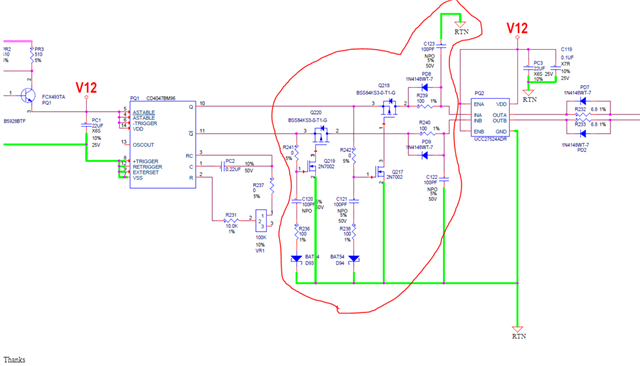
Dear Team,
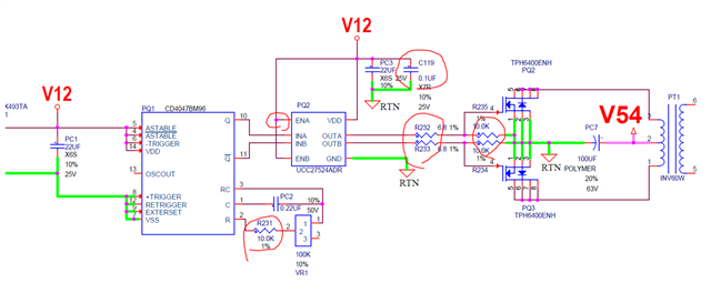
Could you help to check the schematic as below?
it's a inverter application.
Spec:
Vin 12V Vout :54V ac 60W

Many Thanks,
Jimmy
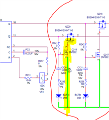
Dear Team,
Could you help to check the schematic as below?
it's a inverter application.
Spec:
Vin 12V Vout :54V ac 60W
Many Thanks,
Jimmy