


Other Parts Discussed in Thread: SN74LXC8T245
We are using the SN74LVC4245A for controlling 5V output logic signals and we have found an issue during power-up.
The component is configured to shift 3.3V logic signals from its side B (VCCB= 3.3V) to its side A (VCCA= 5V). The DIR pin is set to GND and the OE pin is tied to the 5V by a 4.7K resistor (as suggested into datasheet). A regulator supplies the 3.3V from the 5V. 10K resistors pull down all the outputs of the comp (side A).
- At Power up the 5V ramps first, consequently the OE pin ramps too.
- Second, the 3.3V starts several milliseconds after.
- Finally, an open collector transistor asserts the OE pin low.
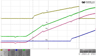
This configuration work properly in many cases. Nevertheless, we have observed an issue when a residual 0.3V voltage persists on the 3.3v rail before the power up (due to a rapid power-off and power-on sequence). In this case, side A outputs are all wrongly activated and ramp with the 5V, until the 3.3V starts to ramp, and despite the pull up resistor on the OE pin.
Unfortunately, this issue create a harmful “flash” behavior on our outputs, which must remain low when powering up.
For example, see Activation of A7 below.
Could you indicate the reasons for this output activation in spite of OE pin state?
Could you suggest modification to solve this problem?
Thanks
