Greetings !
We have problem in our design. Some 5-10% of devices have broken logic buffer SN74LVC2G17DSFR.
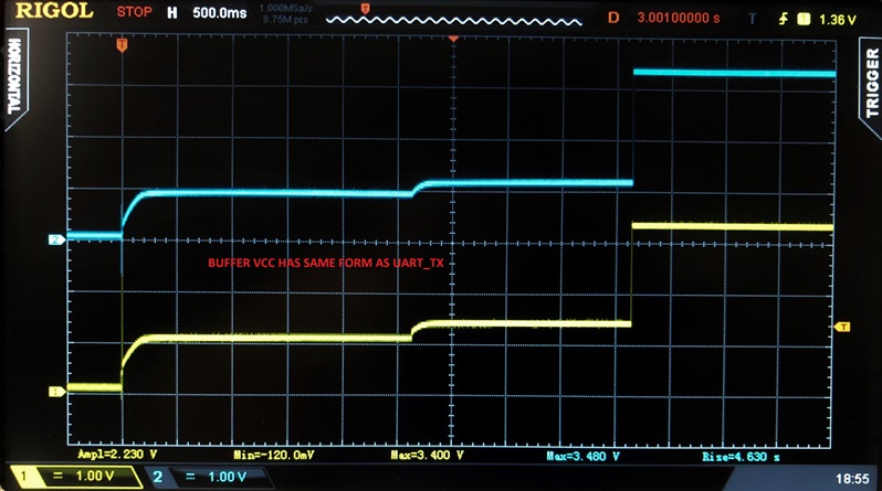
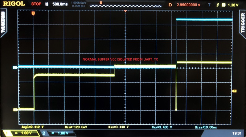
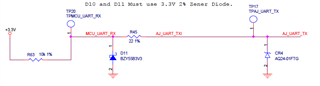
I have several possible variants what's going on. Device has UART and power supplied through 2.5m cable, marked as hot plug on picture with ESD protection on input.
Can you please advice if some of these variants can lead to device fail ?
1) Our logic and microcontroller (uC) on board have power supply that goes wired with UART in one cable.
We have moment during power on (several seconds or more) where Vcc power for logic IC is not available yet but output pin 1Y(AJ_UART_TX) already have around 3.3 V on it.
So could it be violation of design which can lead to device destruction by output voltage higher than Vcc+0.5 ?
2) Could situation described in p. 1 lead to latch-up of device ?
3) There's possibility of device connection without UART connected - only power. Can it lead to situation when floating or even fixed on some voltage like ~1.5 V input 2A (AJ_UART_RX) will turn on both HIGH and LOW side output MOSFETS and destroy device ? (actually on failed part 2Y output have 9 Ohm resistance to GND)
Also do this IC has some numeration patterns to recognize if it's not fake ?
Thanks Waldemar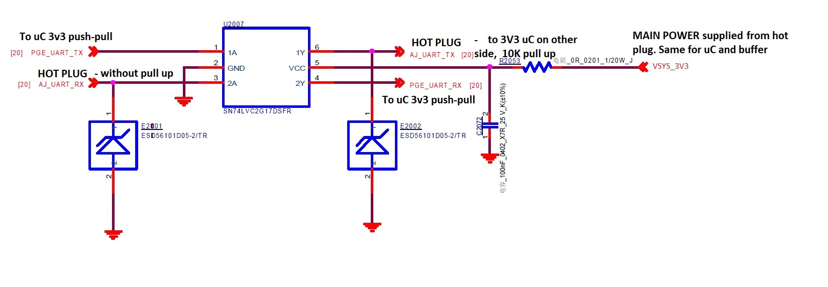

-
Ask a related question
What is a related question?A related question is a question created from another question. When the related question is created, it will be automatically linked to the original question.