Other Parts Discussed in Thread: SN74LVC827A, SN74AUC16244, SN74AUC244, SN74AUCH16244, SN74AUCH244
My customer request to translate 10 bits from 2.5V FPGA to 1.8V,
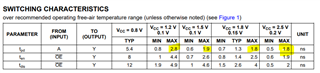
I suggest the SN74LVC16T245 due to >100Mbps data rate, assuming I can leave the extra 6 bits unused.
in total, there is 1 clock bit at 100MHz and 9 data bits (under 100MHz)
questions are:
in SN74LVC16T245
1. assuming my clock is 100MHz, do the other inputs need to share the remaining100Mbps? or are the other bits forced to operate at 100MHz?
2 do all input bits change at the maximum data rate?
another option I suggested was SN74LVC827A 10 bit buffer, for which I would ask the same questions, and in addition: will SN74LVC827A support 2.5V --> 1.8V at 150MHz?