Hi Sir,
My customer would like design CD4504BPWR.
Would you please review parameters and provide your comment?
Conditions:
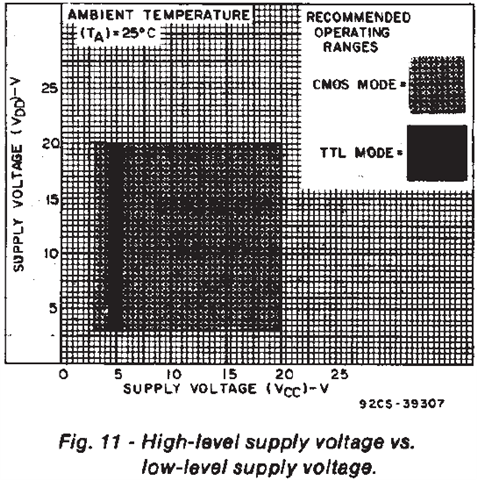
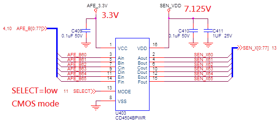
Vcc=3.3V
Vdd=7.125V
SELECT=Low (CMOS-CMOS)

- What is Vcc spec in datasheet? Only Vdd is available in datasheet.

2. What is the Vih and Voh under below conditions?
Vcc=3.3V
Vdd=7.125V
SELECT=Low (CMOS-CMOS)
BR,
SHH