Hi Team,
My customer designed this chip but their layout engineer has some design questions and need our explanation.
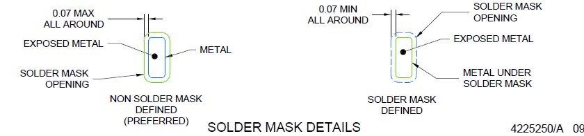
1. On datasheet page 30, as shown in the figure below. There are pin solder mask design with different outline, one is 0.07max, the other is 0.07min. What is the difference between the two outline definition?
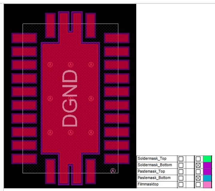
2. On Page 31 of the datasheet shows that the solder mask is an inner green box (left in the figure below), what is the blue outside? And from our EVM's BRD file (right in the figure below) has a pastemask inside and a solder mask outside. Which one is correct?
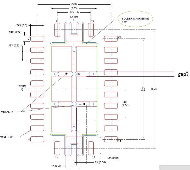
3. In addition, on page 31 of the datasheet, what is the gap of the red boxes inside the IC (marked by the purple line)?
Thanks