Other Parts Discussed in Thread: TINA-TI
Hi,
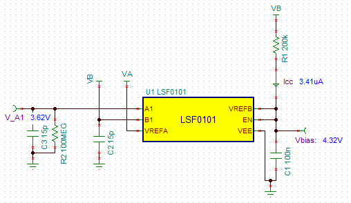
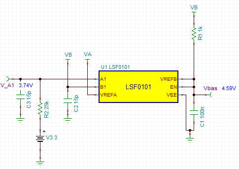
Schematic is attached.
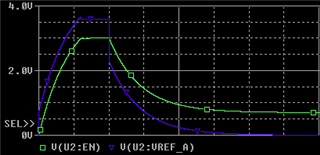
We have VrefA set to approx 3.6V and VrefB set to 5V. We measure "solid" rails at these voltages.
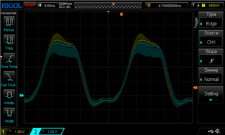
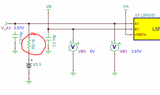
However, VrefB and EN at the LSF0108 chip (Pins 19 and 20) which are "driven" by the 200K/0.1uFD network "droops" to a significant lower voltage when doing data transfers.......as low as about 2V. With no data transfers, we are seeing about 4.5V (ie, about 500mv less than the 5V VrefB). This is causing erroneous PCI transfers.
Somehow the transfer activity is "feeding through" to the Vreb/EN inputs of the LSF0108 chips.
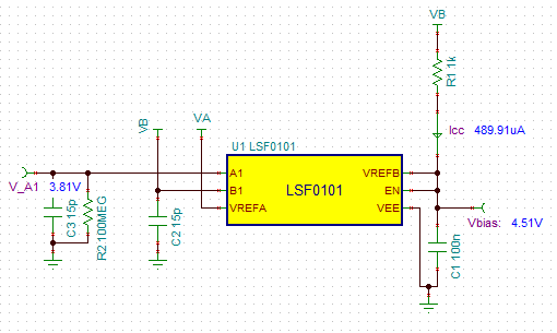
Can we reduce the 200K to something significantly smaller? The LM4051ADJ shut regulator should be able to "sink" whatever current is required through the reference FET.
The purpose of this circuit is to "limit" 5V PCI transfers (VIO = 5V) to 3.6V so as not to blow out the FPGA that is on another page. The FPGA handles the PCI transfers.
We like the series FET style level translators, since they are essentially zero-delay devices.
We like the LSF0108 because it has the internal FET "calibration reference" establishing a precise "threshold voltage" based on the 3.6V VrefA. That is, the FPGA should not see a voltage greater than 3.6V, which is OK for this FPGA.
But, we don't understand why the VrefB/EN to the chip (pins 19 and 20) are not stable during data transfers!
RSVP to advise. You probably need to get the chip designer involved to explain this. We reviewed your excellent videos on the "LSF" family operation, but it's not telling us why we are seeing what we are seeing!!
Thank You,
Joe Norrisschema_lsf0108.pdflsf0108.pdf