Part Number: TXS02612
Hi team,
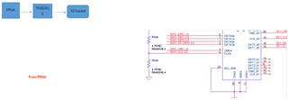
The picture below shows the customer's current architecture, the current PCB layout, the FPGA is far from the TXS02612, and the TXS02612 to the SD socket is relatively close. Considering that the signal trace from FPGA to TXS02612 is a bit long, but looking at the TXS02612 specification (link below), there is no mention of Layout rules. So my customer would like to ask, is there an equal length requirement for the traces of the DATA/CLK/CMD input/output of the TXS02612? Is there a length limit? What is the impedance control of the traces?
https://www.ti.com/lit/gpn/txs02612