Part Number: SN74HC245
Hi Team,
Do we have buffer that can support negative input? Our signal input is -1V and 3.3V and our required output is 0V and 3.3V
Roy
This thread has been locked.
If you have a related question, please click the "Ask a related question" button in the top right corner. The newly created question will be automatically linked to this question.
If you use a series resistor to limit the current to an allowed value (< 20 mA for this device), then it can work. Please not that the clamp current flows out of GND, so the power supply must be able to source that current out of GND.
If you have a negative power supply, you can use comparators.
Hi Roy,
The input voltage may be negative as long as the maximum input current remains < 20mA.


As Clemens stated, the clamp current flows out of GND so the power supply must be able to source that current out of GND.
Regards,
Sebastian
Hi Clemens, Sebastian,
Thank you for your information. For below sentence, I'm not sure about the meaning. For power source, how can I check whether power source can support this feature or not.
the clamp current flows out of GND so the power supply must be able to source that current out of GND.
Regards,
Roy
Hi Roy,
This depends on the current your power supply can source. Can I see a schematic of your design so I can further assist you?
Regards,
Sebastian
Hi Roy,
This could work but you would have to limit the current at the input pin to less than 20mA. Although it is possible I would not recommend applying negative input voltages on our logic devices as we can't guarantee functional operation at specs outside of the recommended operating conditions. I would suggest using a comparator for the negative input so the input signal won't be cutoff below 0V.
Regards,
Sebastian
Hi Sebastian,
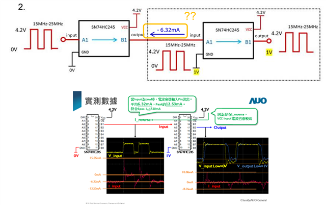
I discussed with customer today. Below is our latest requirement. Can you let me know if there is any side effect for this structure?

Regards,
Roy
Hi Roy,
I would suggest using a series resistor to limit the current on the input of the second SN74HC245. As discussed in the replies above the input current must remain under 20mA, I would suggest starting with a 1kΩ resistor to keep the current well below 20mA.
Regards,
Sebastian
Hi Sebastian,
We did some measurements. And another question is that we found there is -6.32mA on the trace and the direction of current is 2nd buffer A1 to 1st buffer B1. Below are my concerns.
1. Is there any side effect for the current?
2. How can we explain the current path? Because I assume the A1-GND doesn't have ESD diode and so I have no idea the chip internal path of the current.

Regards,
Roy
There is an ESD diode from GND to the input. A current flows from 1 V through the diode, out of A1, into B1, and into 0 V. This current is limited only by the output impedance of B1.
You should add a series resistor between B1 and A1.
Hi Ladisch,
May I double check if our structure is ok for chip or not?
Regards,
Roy
Hi Ladisch,
Our 1V voltage is sink feature. So in your idea, we may need another 1V power supply to source the current out of GND, is it correct?
Please not that the clamp current flows out of GND, so the power supply must be able to source that current out of GND.

Regards,
Roy
Hi Ladisch,
Thank you for your information.
In our structure, we use 1V not only for buffer but also driver circuit. If we place 1kohm, it may impact the driver circle. In my opinion, when LED on, the current path should be red(1V power will be sink) and LED off, current path should be blue(1V power will be source)

And for our measurements, current in/out buffer were in +/-20mA. I think it should be ok. Can you help confirm it without using series 1kohm between 1V and buffer? Thank you.
Regards,
Roy
Hi Roy,
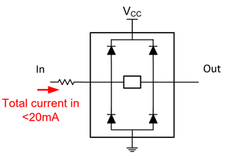
Below is a simplfied example of the clamp diodes on this device. If you place a resistor to limit the current at the input you won't have to worry about current flowing to Vcc.
