Dear Team,
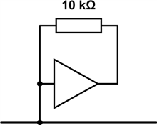
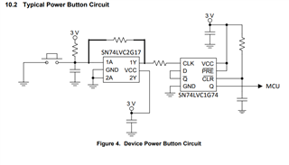
We require one BUS hold circuit for holding two GPIOs in the same state.
Please suggest the part which is having the following requirements.
GPIOs support -2nos
Supply Voltage -3.3V
Regards,
Chitharanjan
Dear Team,
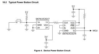
We require one BUS hold circuit for holding two GPIOs in the same state.
Please suggest the part which is having the following requirements.
GPIOs support -2nos
Supply Voltage -3.3V
Regards,
Chitharanjan