Other Parts Discussed in Thread: TXB0104
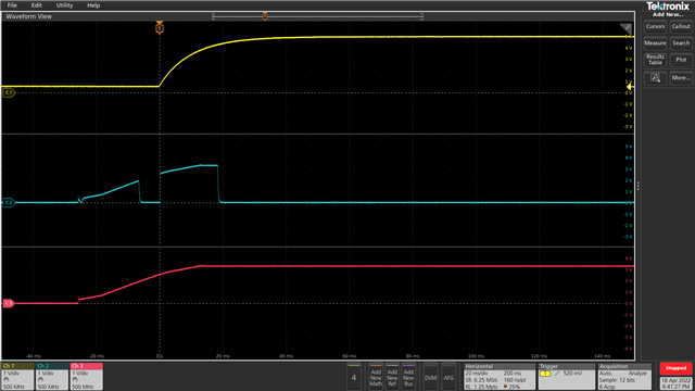
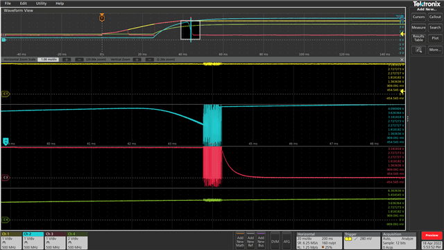
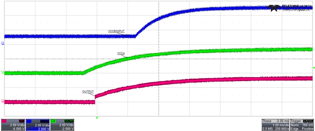
I'm using several TXU0104 devices to interface between 5V logic and 3.3V FPGA IO. In all cases the OE input is tied directly to VCCB. Shifting up, where VCCA == 3.3V and VCCB == 5V works as expected. However, shifting down, where VCCA == 5V and VCCB == 3.3V does not. In the latter case inputs with acceptable logic "1" levels do not generate suitable "1" levels on the B side. I have verified that the part is properly grounded, and that VCCA, VCCB, and OE are connected as expected. I have also verified that nothing is forcing the outputs low. In my bench test the outputs are actually disconnected from the FPGA load. Is there some other requirement that I've somehow missed in the data sheet?