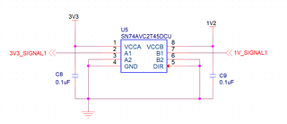
Other Parts Discussed in Thread: SN74AUP1T34, SN74AXC1T45
Hi guys,
I want to know if you can help me to understand if this IC can tolerate and handle the input pins(B) has a different logic level than the voltage supplied through VCCB?.
Basically what I need, is to convert a protocol signal that has 1V logic into 3.3V, I don't have any 1.0V rail on my board, so I want to know if I can supply 1.2V into VCCB instead of the 1.0V that has my I/Os on 'B' side(please see the screenshot) and if this IC can support this configuration or not.
From my understanding VCCA and VCCB can go low as 1.2V, and the datasheet mentioned the I/Os pins can handle signals from -0.5V up to 4.6V, so I don't know if what I want to do with this IC is possible or not (without adding a 1V regulator to my board).
I never seen any of this before on any design(different voltage on VCCA/B than the one I'm having on that I/O) and from my understanding, VCC should be of the same level than the one I'm having on the I/O's Side, but eventhough I just want to confirm this with you guys...
Thanks.


