Hi Experts,
Good day. Seeking advise for SN74HC14 with RC ckt application:
I am using this device SN74HC14. An RC circuit is connected to the input. How should I design RC circuit?
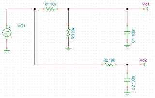
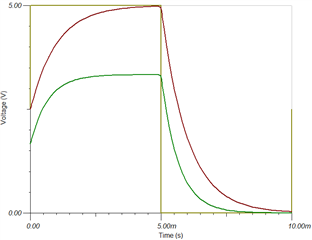
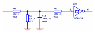
Please find below the RC circuit arrangement connected to the input of SN74HC14. Some values are shown on the circuits. Could we have some equations, notes, etc. to verify those values?
Thank you.
Regards,
Archie A.