Other Parts Discussed in Thread: SN74HC14
Hello Sir/Madam,
My name is Junesang Lee, responsible for EDA simulation in Altair engineering.
I'm writing you because I'd like to ask about things where I got in trouble with the spice model(SN74AUP2G14.cir). Just to put the more information, I compared two cases in the simulation tool below,
Case1: SN74HC14.cir <-- running well
Case2: SN74AUP2G14.cir <-- failed
So, it would be great if someone/expert could take a look at the problem. And two spice models and a description(.pptx) including questions have been attached. Please refer to them. Thank you!
[SN74AUP2G14]Spice simulation problem.pptx
********************************************************************************
* SN74HC14.cir
* 2.0
* 2019-11-14 00:00:00
* Texas Instruments Incorporated.
* Standard Logic, SLHR
* 12500 TI Blvd
* Dallas, TX -75243
*
* Revision History:
* Rev 2.0: 01/01/2019
* - Model generated from datasheet values
* - Built using generic logic gate behavioral pspice model V2
* - Built using an automated model which generalizes parts under same family
* - Performance is expected typical behavior at 25C
* - Written for and tested with Tina-TI Version 9.3.100.244 SF-TI
* - Accurate power consumption with dyanmic as well as static Icc
*
********************************************************************************
*[Disclaimer]
* This model is designed as an aid for customers of Texas Instruments.
* TI and its licensors and suppliers make no warranties, either expressed
* or implied, with respect to this model, including the warranties of
* merchantability or fitness for a particular purpose. The model is
* provided solely on an "as is" basis. The entire risk as to its quality
* and performance is with the customer.
*
*[Copyright]
*(C) Copyright 2019 Texas Instruments Incorporated.All rights reserved.
*
*
********************************************************************************
* SN74HC14
********************************************************************************
.SUBCKT SN74HC14 A Y VCC AGND ENABLE
XU1 Y A VCC VCC AGND LOGIC_GATE_2PIN_OD_HC_1i_NAND_PP_ST_SN74HC14
.ENDS
.SUBCKT LOGIC_GATE_2PIN_OD_HC_1i_NAND_PP_ST_SN74HC14 OUT A B VCC GND
.PARAM VCC_ABS_MAX = 7
.PARAM VCC_MAX = 6
.PARAM RA = 240000000
.PARAM RB = 240000000
.PARAM CA = 1e-11
.PARAM CB = 1e-11
.PARAM ROEZ = 5000
.PARAM COEZ = 3e-12
RA A GND {RA}
RB B GND {RB}
CA A GND {CA}
CB B GND {CB}
XUA NA A VCC GND LOGIC_INPUT_HC_1i_NAND_PP_ST_SN74HC14
XUB NB B VCC GND LOGIC_INPUT_HC_1i_NAND_PP_ST_SN74HC14
XUG NA NB NOUTG VCC GND LOGIC_FUNCTION_2_HC_1i_NAND_PP_ST_SN74HC14
XOUTPD NOUTG NOUTTPD VCC GND TPD_HC_1i_NAND_PP_ST_SN74HC14
XUOUT NOUTTPD NOUT_INT VCC GND LOGIC_PP_OUTPUT_HC_1i_NAND_PP_ST_SN74HC14
XICC VCC GND NVIOUT LOGIC_ICC_HC_1i_NAND_PP_ST_SN74HC14
SICC VCC GND VCC GND SW1
H1 NVIOUT GND VIOUT 1
VIOUT NOUT_INT OUTsw 0
SIOFF OUTsw OUT VCC GND SW2
DA2 GND A D1
DB2 GND B D1
DO2 GND OUT D1
RDA1 NA1 GND 1e6
SDA1 NA1 A VCC GND SW2
RDB1 NB1 GND 1e6
SDB1 NB1 B VCC GND SW2
RDO1 NO1 GND 1e6
SDO1 NO1 OUT VCC GND SW2
.MODEL SW1 VSWITCH VON = {VCC_ABS_MAX} VOFF = {VCC_MAX} RON = 10 ROFF = 60e6
.MODEL SW2 VSWITCH VON = {0.55} VOFF = {0.45} RON = 10m ROFF = 100e6
.MODEL D1 D
.ENDS
.SUBCKT LOGIC_INPUT_HC_1i_NAND_PP_ST_SN74HC14 OUT IN VCC VEE
.PARAM STANDARD_INPUT_SELECT = 0
.PARAM SCHMITT_TRIGGER_INPUT_SELECT = 1
ESTD_THR VSTD_THR VEE TABLE {V(VCC,VEE)} =
+(1,0.5)
+(1.8,0.9)
+(2.5,1.25)
+(3.3,1.65)
+(5,2.5)
+(6,3)
ETRP_P VTRP_P VEE TABLE {V(VCC,VEE)} =
+(2,1.2)
+(4.5,2.5)
+(6,3.3)
ETRP_N VTRP_N VEE TABLE {V(VCC,VEE)} =
+(2,0.6)
+(4.5,1.6)
+(6,2)
EHYST VHYST VEE TABLE {V(VCC,VEE)} =
+(2,0.6)
+(4.5,0.9)
+(6,1.3)
ETRUE NTRUE VEE VALUE = {V(VCC,VEE)}
EFALSE NFALSE VEE VALUE = {0}
EBETA BETA VEE VALUE = {V(VHYST,VEE)/(V(NTRUE,VEE) - V(NFALSE,VEE) + V(VHYST,VEE))}
EFB NFB VEE VALUE = {(1 - V(BETA,VEE))*V(IN,VEE) + V(BETA,VEE)*V(CURR_OUT,VEE)}
EREF NREF VEE VALUE = {0.5*(1 - V(BETA,VEE))*(V(VTRP_P,VEE) + V(VTRP_N,VEE))
+ + 0.5*V(BETA,VEE)*(V(NTRUE,VEE) + V(NFALSE,VEE))}
EDIFF NDIFF VEE VALUE = {V(NFB,NREF)}
ESWITCH VSWITCH VEE VALUE = {0.5*(-SGN(V(NDIFF,VEE)) + ABS(SGN(V(NDIFF,VEE))))}
ESWITCH1 VSWITCH1 VEE VALUE = {0.5*(SGN(V(NDIFF,VEE)) + ABS(SGN(V(NDIFF,VEE))))}
GCOMP VEE CURR_OUT VALUE = {SCHMITT_TRIGGER_INPUT_SELECT*0.5*V(VCC,VEE)*(SGN(V(NDIFF,VEE)) + ABS(SGN(V(NDIFF,VEE))))}
GSTD VEE CURR_OUT VALUE = {STANDARD_INPUT_SELECT*0.5*V(VCC,VEE)*(SGN(V(IN,VSTD_THR)) + ABS(SGN(V(IN,VSTD_THR))))}
ROUT CURR_OUT VEE 1
EMID MID VEE VALUE = {0.5*(V(VCC,VEE) + V(VEE))}
EARG NARG VEE VALUE = {V(CURR_OUT,VEE) - V(MID,VEE)}
EOUT OUT VEE VALUE = {0.5*(SGN(V(NARG,VEE)) + ABS(SGN(V(NARG,VEE) ) ) )}
.PARAM MAXICC = 0.0009
.PARAM VT = .7
.PARAM VCC_MIN = 2
EV_VT1 VTN VEE VALUE = { VT }
EV_VT2 VTP VEE VALUE = { V(VCC,VEE) - VT }
ETEST TEST VEE VALUE = {.9*V(VCC,VEE)}
EVTHDIFF VTH_DIFF VEE VALUE = {V(IN,VSTD_THR)}
EVTHPDIFF VTHP_DIFF VEE VALUE = {V(IN,VTRP_P)}
EVTHNDIFF VTHN_DIFF VEE VALUE = {V(IN,VTRP_N)}
EVTNDIFF VTN_DIFF VEE VALUE = { V(IN,VTN) }
EVTPDIFF VTP_DIFF VEE VALUE = { V(IN,VTP) }
GICCVA VCC VEE VALUE = { (-ABS(( (1+SGN(V(VTN_DIFF,VEE)) ) )/2 -1) *
+ 2*MAXICC*((V(IN,VEE)-VT)/V(VCC,VEE))^2)*(1 + SGN(V(VCC,VEE) - VCC_MIN))*V(VSWITCH,VEE)}
GICCVB VCC VEE VALUE = { (ABS(( (1+SGN(V(VTHP_DIFF,VEE)) ) )/2 -1) *
+ 2*MAXICC*((V(IN,VEE)-VT)/V(VCC,VEE))^2)*(1 + SGN(V(VCC,VEE) - VCC_MIN))*V(VSWITCH,VEE)}
GICCVC VCC VEE VALUE = { ( ABS( (1+SGN(V(VTHN_DIFF,VEE)) ) )/2 *
+ 2*MAXICC*((V(IN,VEE)-(V(VCC,VEE)-VT))/V(VCC,VEE))^2)*(1 + SGN(V(VCC,VEE) - VCC_MIN))*V(VSWITCH1,VEE)}
GICCVD VCC VEE VALUE = { (-ABS( (1+SGN(V(VTP_DIFF,VEE)) ) )/2 *
+ 2*MAXICC*((V(IN,VEE)-(V(VCC,VEE)-VT))/V(VCC,VEE))^2)*(1 + SGN(V(VCC,VEE) - VCC_MIN))*V(VSWITCH1,VEE)}
.ENDS
.SUBCKT LOGIC_FUNCTION_2_HC_1i_NAND_PP_ST_SN74HC14 A B OUT VCC VEE
.PARAM AND = 0
.PARAM NAND = 1
.PARAM OR = 0
.PARAM NOR = 0
.PARAM XOR = 0
.PARAM XNOR = 0
GAND VEE N1 VALUE = {AND*V(A,VEE)*V(B,VEE)}
GNAND VEE N1 VALUE = {NAND*(1 - V(A,VEE)*V(B,VEE))}
GOR VEE N1 VALUE = {OR*(MIN(V(A,VEE) + V(B,VEE),1))}
GNOR VEE N1 VALUE = {NOR*(1 - MIN(V(A,VEE) + V(B,VEE),1))}
GXOR VEE N1 VALUE = {XOR*((1 - V(A,VEE))*V(B,VEE) + V(A,VEE)*(1 - V(B,VEE)))}
GXNOR VEE N1 VALUE = {XNOR*(1 - ((1 - V(A,VEE))*V(B,VEE) + V(A,VEE)*(1 - V(B,VEE))))}
RN1 N1 VEE 1
EOUT OUT VEE N1 VEE 1
.ENDS
.SUBCKT TPD_HC_1i_NAND_PP_ST_SN74HC14 IN OUT VCC VEE
.PARAM TPDELAY1 = 1N
.PARAM RS = 10K
.PARAM CS = {-TPDELAY1/(RS*LOG(0.5))}
ETPDNORM NTPDNORM VEE TABLE {V(VCC,VEE)} =
+(2,90)
+(4.5,18.5)
+(6,16)
G1 IN N1 VALUE = {V(IN,N1)/(V(NTPDNORM,VEE)*RS)}
RZ IN N1 10G
C1 N1 VEE {CS}
E1 N2 VEE VALUE = {0.5*(1 + SGN(V(N1,VEE) - 0.5))}
EOUT OUT VEE N2 VEE 1
.ENDS
.SUBCKT LOGIC_PP_OUTPUT_HC_1i_NAND_PP_ST_SN74HC14 IN OUT VCC VEE
EROH NROH VEE TABLE {V(VCC,VEE)} =
+(2,3000)
+(4.5,30)
+(6,23.0769230769231)
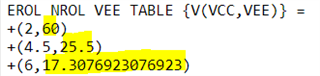
EROL NROL VEE TABLE {V(VCC,VEE)} =
+(2,60)
+(4.5,25.5)
+(6,17.3076923076923)
E1 N1 VEE VALUE = {V(VCC,VEE)*V(IN,VEE)}
GOUT N1 OUT VALUE = {V(N1,OUT)*(V(IN,VEE)/V(NROH,VEE) + (1 - V(IN,VEE))/V(NROL,VEE))}
.ENDS
.SUBCKT LOGIC_ICC_HC_1i_NAND_PP_ST_SN74HC14 VCC VEE VIOUT
.PARAM ICC = 2.5e-07
.PARAM VCC_MAX = 6
.PARAM VCC_MIN = 2
GICC VCC VEE VALUE = {ICC*0.5*(1 + SGN(V(VCC,VEE) - VCC_MIN))}
EGNDF GNDF 0 VALUE = {0.5*(V(VCC) + V(VEE))}
GOUTP VCC GNDF VALUE = {V(VIOUT,VEE)*0.5*(SGN(V(VIOUT,VEE)) + ABS(SGN(V(VIOUT,VEE))))}
GOUTN GNDF VEE VALUE = {V(VIOUT,VEE)*0.5*(SGN(V(VIOUT,VEE)) + ABS(SGN(V(VIOUT,VEE))))}
.ENDS
********************************************************************************
* SN74AUP2G14.cir
* 2.0
* 2019-11-15 00:00:00
* Texas Instruments Incorporated.
* Standard Logic, SLHR
* 12500 TI Blvd
* Dallas, TX -75243
*
* Revision History:
* Rev 2.0: 01/01/2019
* - Model generated from datasheet values
* - Built using generic logic gate behavioral pspice model V2
* - Built using an automated model which generalizes parts under same family
* - Performance is expected typical behavior at 25C
* - Written for and tested with Tina-TI Version 9.3.100.244 SF-TI
* - Accurate power consumption with dyanmic as well as static Icc
*
********************************************************************************
*[Disclaimer]
* This model is designed as an aid for customers of Texas Instruments.
* TI and its licensors and suppliers make no warranties, either expressed
* or implied, with respect to this model, including the warranties of
* merchantability or fitness for a particular purpose. The model is
* provided solely on an "as is" basis. The entire risk as to its quality
* and performance is with the customer.
*
*[Copyright]
*(C) Copyright 2019 Texas Instruments Incorporated.All rights reserved.
*
*
********************************************************************************
* SN74AUP2G14
********************************************************************************
.SUBCKT SN74AUP2G14 A Y VCC AGND ENABLE
XU1 Y A VCC VCC AGND LOGIC_GATE_2PIN_OD_AUP_1i_NAND_PP_ST_SN74AUP2G14
.ENDS
.SUBCKT LOGIC_GATE_2PIN_OD_AUP_1i_NAND_PP_ST_SN74AUP2G14 OUT A B VCC GND
.PARAM VCC_ABS_MAX = 4.6
.PARAM VCC_MAX = 3.6
.PARAM RA = 1440000000
.PARAM RB = 1440000000
.PARAM CA = 1.5e-12
.PARAM CB = 1.5e-12
.PARAM ROEZ = 173.68421052631572
.PARAM COEZ = 3e-12
RA A GND {RA}
RB B GND {RB}
CA A GND {CA}
CB B GND {CB}
XUA NA A VCC GND LOGIC_INPUT_AUP_1i_NAND_PP_ST_SN74AUP2G14
XUB NB B VCC GND LOGIC_INPUT_AUP_1i_NAND_PP_ST_SN74AUP2G14
XUG NA NB NOUTG VCC GND LOGIC_FUNCTION_2_AUP_1i_NAND_PP_ST_SN74AUP2G14
XOUTPD NOUTG NOUTTPD VCC GND TPD_AUP_1i_NAND_PP_ST_SN74AUP2G14
XUOUT NOUTTPD NOUT_INT VCC GND LOGIC_PP_OUTPUT_AUP_1i_NAND_PP_ST_SN74AUP2G14
XICC VCC GND NVIOUT LOGIC_ICC_AUP_1i_NAND_PP_ST_SN74AUP2G14
SICC VCC GND VCC GND SW1
H1 NVIOUT GND VIOUT 1
VIOUT NOUT_INT OUTsw 0
SIOFF OUTsw OUT VCC GND SW2
DA2 GND A D1
DB2 GND B D1
DO2 GND OUT D1
RDA1 NA1 GND 1e6
SDA1 NA1 A VCC GND SW2
RDB1 NB1 GND 1e6
SDB1 NB1 B VCC GND SW2
RDO1 NO1 GND 1e6
SDO1 NO1 OUT VCC GND SW2
.MODEL SW1 VSWITCH VON = {VCC_ABS_MAX} VOFF = {VCC_MAX} RON = 10 ROFF = 60e6
.MODEL SW2 VSWITCH VON = {0.55} VOFF = {0.45} RON = 10m ROFF = 100e6
.MODEL D1 D
.ENDS
.SUBCKT LOGIC_INPUT_AUP_1i_NAND_PP_ST_SN74AUP2G14 OUT IN VCC VEE
.PARAM STANDARD_INPUT_SELECT = 0
.PARAM SCHMITT_TRIGGER_INPUT_SELECT = 1
ESTD_THR VSTD_THR VEE TABLE {V(VCC,VEE)} =
+(1,0.5)
+(1.8,0.9)
+(2.5,1.25)
+(3.3,1.65)
+(5,2.5)
+(6,3)
ETRP_P VTRP_P VEE TABLE {V(VCC,VEE)} =
+(0.8,0.45)
+(1.1,0.715)
+(1.4,0.925)
+(1.65,1.1)
+(2.3,1.57)
+(3,2.085)
ETRP_N VTRP_N VEE TABLE {V(VCC,VEE)} =
+(0.8,0.35)
+(1.1,0.45)
+(1.4,0.57)
+(1.65,0.65)
+(2.3,0.85)
+(3,1.06)
EHYST VHYST VEE TABLE {V(VCC,VEE)} =
+(0.8,0.285)
+(1.1,0.27)
+(1.4,0.37)
+(1.65,0.465)
+(2.3,0.725)
+(3,1.05)
ETRUE NTRUE VEE VALUE = {V(VCC,VEE)}
EFALSE NFALSE VEE VALUE = {0}
EBETA BETA VEE VALUE = {V(VHYST,VEE)/(V(NTRUE,VEE) - V(NFALSE,VEE) + V(VHYST,VEE))}
EFB NFB VEE VALUE = {(1 - V(BETA,VEE))*V(IN,VEE) + V(BETA,VEE)*V(CURR_OUT,VEE)}
EREF NREF VEE VALUE = {0.5*(1 - V(BETA,VEE))*(V(VTRP_P,VEE) + V(VTRP_N,VEE))
+ + 0.5*V(BETA,VEE)*(V(NTRUE,VEE) + V(NFALSE,VEE))}
EDIFF NDIFF VEE VALUE = {V(NFB,NREF)}
ESWITCH VSWITCH VEE VALUE = {0.5*(-SGN(V(NDIFF,VEE)) + ABS(SGN(V(NDIFF,VEE))))}
ESWITCH1 VSWITCH1 VEE VALUE = {0.5*(SGN(V(NDIFF,VEE)) + ABS(SGN(V(NDIFF,VEE))))}
GCOMP VEE CURR_OUT VALUE = {SCHMITT_TRIGGER_INPUT_SELECT*0.5*V(VCC,VEE)*(SGN(V(NDIFF,VEE)) + ABS(SGN(V(NDIFF,VEE))))}
GSTD VEE CURR_OUT VALUE = {STANDARD_INPUT_SELECT*0.5*V(VCC,VEE)*(SGN(V(IN,VSTD_THR)) + ABS(SGN(V(IN,VSTD_THR))))}
ROUT CURR_OUT VEE 1
EMID MID VEE VALUE = {0.5*(V(VCC,VEE) + V(VEE))}
EARG NARG VEE VALUE = {V(CURR_OUT,VEE) - V(MID,VEE)}
EOUT OUT VEE VALUE = {0.5*(SGN(V(NARG,VEE)) + ABS(SGN(V(NARG,VEE) ) ) )}
.PARAM MAXICC = 0.0009
.PARAM VT = .7
.PARAM VCC_MIN = 0.8
EV_VT1 VTN VEE VALUE = { VT }
EV_VT2 VTP VEE VALUE = { V(VCC,VEE) - VT }
ETEST TEST VEE VALUE = {.9*V(VCC,VEE)}
EVTHDIFF VTH_DIFF VEE VALUE = {V(IN,VSTD_THR)}
EVTHPDIFF VTHP_DIFF VEE VALUE = {V(IN,VTRP_P)}
EVTHNDIFF VTHN_DIFF VEE VALUE = {V(IN,VTRP_N)}
EVTNDIFF VTN_DIFF VEE VALUE = { V(IN,VTN) }
EVTPDIFF VTP_DIFF VEE VALUE = { V(IN,VTP) }
GICCVA VCC VEE VALUE = { (-ABS(( (1+SGN(V(VTN_DIFF,VEE)) ) )/2 -1) *
+ 2*MAXICC*((V(IN,VEE)-VT)/V(VCC,VEE))^2)*(1 + SGN(V(VCC,VEE) - VCC_MIN))*V(VSWITCH,VEE)}
GICCVB VCC VEE VALUE = { (ABS(( (1+SGN(V(VTHP_DIFF,VEE)) ) )/2 -1) *
+ 2*MAXICC*((V(IN,VEE)-VT)/V(VCC,VEE))^2)*(1 + SGN(V(VCC,VEE) - VCC_MIN))*V(VSWITCH,VEE)}
GICCVC VCC VEE VALUE = { ( ABS( (1+SGN(V(VTHN_DIFF,VEE)) ) )/2 *
+ 2*MAXICC*((V(IN,VEE)-(V(VCC,VEE)-VT))/V(VCC,VEE))^2)*(1 + SGN(V(VCC,VEE) - VCC_MIN))*V(VSWITCH1,VEE)}
GICCVD VCC VEE VALUE = { (-ABS( (1+SGN(V(VTP_DIFF,VEE)) ) )/2 *
+ 2*MAXICC*((V(IN,VEE)-(V(VCC,VEE)-VT))/V(VCC,VEE))^2)*(1 + SGN(V(VCC,VEE) - VCC_MIN))*V(VSWITCH1,VEE)}
.ENDS
.SUBCKT LOGIC_FUNCTION_2_AUP_1i_NAND_PP_ST_SN74AUP2G14 A B OUT VCC VEE
.PARAM AND = 0
.PARAM NAND = 1
.PARAM OR = 0
.PARAM NOR = 0
.PARAM XOR = 0
.PARAM XNOR = 0
GAND VEE N1 VALUE = {AND*V(A,VEE)*V(B,VEE)}
GNAND VEE N1 VALUE = {NAND*(1 - V(A,VEE)*V(B,VEE))}
GOR VEE N1 VALUE = {OR*(MIN(V(A,VEE) + V(B,VEE),1))}
GNOR VEE N1 VALUE = {NOR*(1 - MIN(V(A,VEE) + V(B,VEE),1))}
GXOR VEE N1 VALUE = {XOR*((1 - V(A,VEE))*V(B,VEE) + V(A,VEE)*(1 - V(B,VEE)))}
GXNOR VEE N1 VALUE = {XNOR*(1 - ((1 - V(A,VEE))*V(B,VEE) + V(A,VEE)*(1 - V(B,VEE))))}
RN1 N1 VEE 1
EOUT OUT VEE N1 VEE 1
.ENDS
.SUBCKT TPD_AUP_1i_NAND_PP_ST_SN74AUP2G14 IN OUT VCC VEE
.PARAM TPDELAY1 = 1N
.PARAM RS = 10K
.PARAM CS = {-TPDELAY1/(RS*LOG(0.5))}
ETPDNORM NTPDNORM VEE TABLE {V(VCC,VEE)} =
+(1.2,8)
+(1.5,5)
+(1.8,4.8)
+(2.5,3.5)
+(3.3,3)
G1 IN N1 VALUE = {V(IN,N1)/(V(NTPDNORM,VEE)*RS)}
RZ IN N1 10G
C1 N1 VEE {CS}
E1 N2 VEE VALUE = {0.5*(1 + SGN(V(N1,VEE) - 0.5))}
EOUT OUT VEE N2 VEE 1
.ENDS
.SUBCKT LOGIC_PP_OUTPUT_AUP_1i_NAND_PP_ST_SN74AUP2G14 IN OUT VCC VEE
EROH NROH VEE TABLE {V(VCC,VEE)} =
+(1.1,150)
+(1.4,102.352941176471)
+(1.65,104.210526315789)
+(2.3,103.896103896104)
+(3,60)
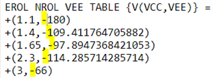
EROL NROL VEE TABLE {V(VCC,VEE)} =
+(1.1,-180)
+(1.4,-109.411764705882)
+(1.65,-97.8947368421053)
+(2.3,-114.285714285714)
+(3,-66)
E1 N1 VEE VALUE = {V(VCC,VEE)*V(IN,VEE)}
GOUT N1 OUT VALUE = {V(N1,OUT)*(V(IN,VEE)/V(NROH,VEE) + (1 - V(IN,VEE))/V(NROL,VEE))}
.ENDS
.SUBCKT LOGIC_ICC_AUP_1i_NAND_PP_ST_SN74AUP2G14 VCC VEE VIOUT
.PARAM ICC = 2.5e-08
.PARAM VCC_MAX = 3.6
.PARAM VCC_MIN = 0.8
GICC VCC VEE VALUE = {ICC*0.5*(1 + SGN(V(VCC,VEE) - VCC_MIN))}
EGNDF GNDF 0 VALUE = {0.5*(V(VCC) + V(VEE))}
GOUTP VCC GNDF VALUE = {V(VIOUT,VEE)*0.5*(SGN(V(VIOUT,VEE)) + ABS(SGN(V(VIOUT,VEE))))}
GOUTN GNDF VEE VALUE = {V(VIOUT,VEE)*0.5*(SGN(V(VIOUT,VEE)) + ABS(SGN(V(VIOUT,VEE))))}
.ENDS