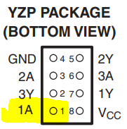
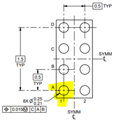
Please clarify pinouts for SN74LVC3G04YZPR in term of BGA ball, A1,A2, B1,B2, C1,C2 and D1, D2.
The datasheets reference the BGA as 1,2,3,4,5,6,7 and 8. The footprints are defined in term of A1,A2 etc. I'd want to make sure there are no mapping issue and need the clarification.
Thanks in advance.


