This thread has been locked.

If you have a related question, please click the "Ask a related question" button in the top right corner. The newly created question will be automatically linked to this question.

CD74HC4046A: PC3OUT OPERATION

Part Number: CD74HC4046A
Other Parts Discussed in Thread: SN74LV4046A

Hello,

I have a question about the data sheet(Data sheet acquired from Harris Semiconductor SCHS204J) of CD74HC4046A.

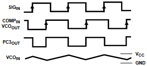
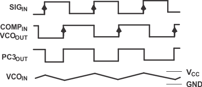
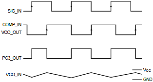
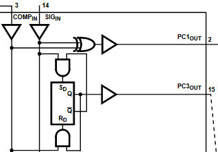
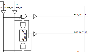
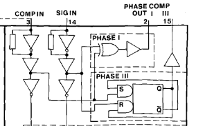
Regarding Phase Comparator 3 (PC3), Figure 7 of the data sheet is an illustration of the operation waveform of PC3. Is this correct?

It seems that SIGIN and COMPIN (VCOOUT) are the opposite compared to the data sheet of other equivalent manufacturers.

  • The PC3 output indeed is inverted:

    CD74HC4046A (Harris):

    SN74LV4046A (TI):

    74HC4046A (Nexperia):

    The functional block diagrams in the Harris and Nexperia datasheets are the same:

    CD74HC4046A:

    74HC4046A:

    But the functional block diagram in the CMOS Phase-Locked-Loop Applications Using the CD54/74HC/HCT4046A and CD54/74HC/HCT7046A application report shows different connections:

    The SN74LV4046A datasheet calls out compatibility with the CD74HC4046A, so I have to conclude that figure 7 is correct, and that the Nexperia device indeed has an inverted output compared to the other manufacturers.

  • I have a feeling that these are all compatible and there is a datasheet error.

    Now there are two points on compatibility... Does PC3_OUT need to have the proper phase vs. inputs -- or just keep things locked?

    My key point of confusion is that the Harris & TI logic block diagrams seem to conflict with their PC3 plots.  The Nexperia shows what I think is the correct waveform.

    The first point on the plot has COMPIN = 1, SIGIN = 0, and PC3_OUT=1.

    Because COMPIN=1 and PC3_OUT=1, then the AND gate feeding the RESET should be asserted and set PC3_OUT=0 immediately.

    I find that this error could exist after so long causing me concern that I'm missing something.  But perhaps not and the Nexperia part simply made the plot correctly.

      --> Does this help?

    --

    The app note is interesting to show the inversions... but it also connects SIGIN to RESET instead of SIGIN to SET.  So that seems to cancel out... and PC1_OUT is XOR so it doesn't care if both inputs are inverted or not.

    73,
    Timothy

  • The RS flip-flop is edge triggered. And all datasheets agree that it is the rising edge (at the pin).

  • Ok sure, it's edge triggered... but what was the state that got to the waveform to the state shown at the beginning?  If PC3_OUT=1, then the next transition of PC3_OUT should occur only when COMPIN goes high which will the reset the flip flop and set PC3_OUT = 0.... but by the diagram PC3_OUT transitions on the next SIGIN rising edge... that's why I'm saying it appears a datasheet error and the Nexperia timing diagram appears to have got it right.

    So while my point about it immediately transitioning may not be right, I don't think the waveform is correct.  Again, unless I'm missing something else.  But I don't know what that is.

    73,
    Timothy

  • Hello everyone,

    After all, is Figure 7 right or wrong?

    For additional information, ON-SEMI has the same waveform as EXPERIA.

    Also, the average voltage rise and fall of VCOIN shown in Fig. 7 are opposite to EXPERIA and ON-SEMI, and are not compatible.

  • This question can be answered only by looking at an actual chip.