Other Parts Discussed in Thread: SN74AUP1G32, SN74AUP1G97
Dear Sir:
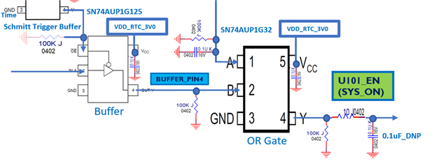
SN74AUP1G125 (Buffer-3 State) output abnormal issue.
1.The input(OE\) of SN74AUP1G125 (Buffer-3 State) is Low.
(1) Rise:
The input(A) of SN74AUP1G125 (Buffer-3 State) rise time doesn't exceed the Δt/Δv Input transition rate max.(200ns/V).
The output(Y) of SN74AUP1G125 (Buffer-3 State) rise time is shorter than the propagation delay.
(2) Fall:
The input(A) of SN74AUP1G125 (Buffer-3 State) fall time doesn't exceed the Δt/Δv Input transition rate max.(200ns/V).
The output(Y) of SN74AUP1G125 (Buffer-3 State) fall time is shorter than the propagation delay.
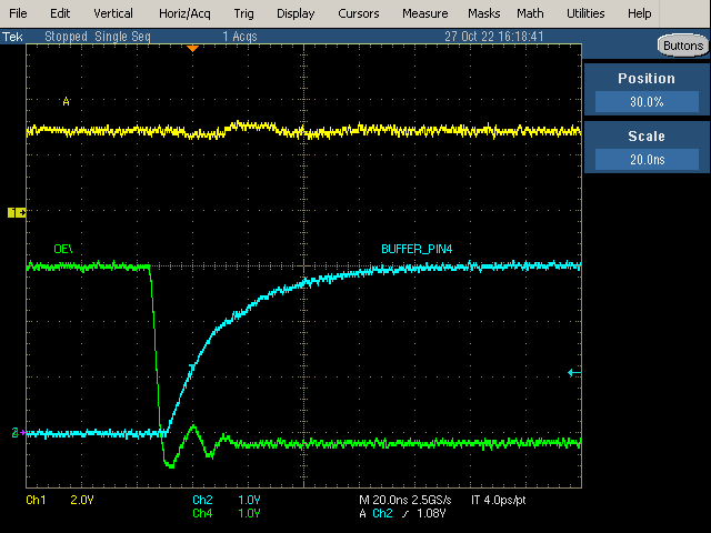
2.The input(A) of SN74AUP1G125 (Buffer-3 State) Keep High.
The input(OE\) of SN74AUP1G125 (Buffer-3 State) change from High to Low.
The input(OE\) of SN74AUP1G125 (Buffer-3 State) doesn't exceed the Δt/Δv Input transition rate max.(200ns/V).
The output(Y)(Buffer Pin4) of SN74AUP1G125 (Buffer-3 State) rise time is shorter than the propagation delay.
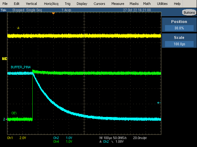
3.The input(A) of SN74AUP1G125 (Buffer-3 State) Keep High.
The input(OE\) of SN74AUP1G125 (Buffer-3 State) change from Low to High.
The input(OE\) of SN74AUP1G125 (Buffer-3 State) doesn't exceed the Δt/Δv Input transition rate max.(200ns/V).
The output(Y)(Buffer Pin4) of SN74AUP1G125 (Buffer-3 State) fall time is longer than the propagation delay.
The fall time is micro-second(us) level very longer.
Why is the output(Y)(Buffer Pin4) of SN74AUP1G125 (Buffer-3 State) fall time so longer?
Is it normal?
Please check to reply it asap.
Thanks a lot.
Best regards
Vincent