


Hello,
Excuse me to insist on this topic, but I still don't understand completely.
According to the logic diagram of the transceiver:
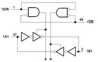
and knowing that it is said in the datasheet that " To ensure the high-impedance state during power up or power down, OE should be tied to VCC through a
pullup resistor",
I still do not understand why tying DIR to VCC would not ensure A output to be high impedance during power up or power down whatever OE level.
Are OE and DIR managed differently inside the chip?
Thank you in advance,
Best regards
Pierre
