A related question is a question created from another question. When the related question is created, it will be automatically linked to the original question.
If you have a related question, please click the "Ask a related question" button in the top right corner. The newly created question will be automatically linked to this question.
The PGA113 was developed and introduced to the market over a decade ago and unfortunately no SPICE model was developed for this part. The best way to get familiar with this device is through our evaluation module PGA113EVM-B. I checked the inventory on ti.com and we do have this evaluation module in stock.
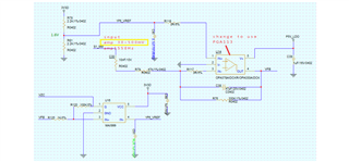
It looks like you are intending to use the PGA113 as a simple programmable gain block to replace the fixed-gain amplifier in your circuit. The PGA113 has some additional features such as an input multiplexer and internal calibration channels that can be used for system-level calibration. Are you looking for a reference design that includes the calibration or multiplexer features?
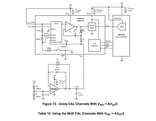
Figure 72 from the PGA113 datasheet shows a typical configuration using the calibration channels. Note that Vcal/CH0 must be connected to the ADC reference potential to use the calibration (in this figure it is connected to AVDD because this is equal to the ADC Ref voltage). The PGA113 VREF pin must be connected to a low-impedance reference capable of sourcing and sinking at least 2mA. Figure 72 shows the OPA364 in a buffer configuration to provide the low-impedance voltage to the VREF pin.
If you do not require the calibration feature you may use the configuration shown above and simply use the multiplexer to select CH1 as your input.
I see your input source is expected to be between 30mV and 500mV at 1550Hz but the schematic does not show what this is referenced to. Is this 30mV-500mV input signal referenced to ground? Or is it referenced to the 1.65V mid-supply?