This thread has been locked.

If you have a related question, please click the "Ask a related question" button in the top right corner. The newly created question will be automatically linked to this question.

SN74HC14: Abnormal output behavior

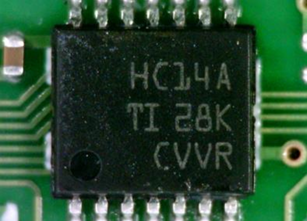
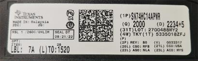
Part Number: SN74HC14

Hi support team.

Recently, we have confirmed many individuals (5pcs, confirmed with multiple lot numbers) that behave abnormally in the products of the new process for which PCNs have been issued by our customers.

A similar phenomenon has not been confirmed even once in the product before the process change.

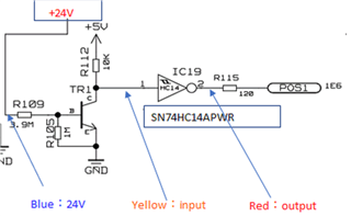
These individuals do not have an input Schmidt trigger function.

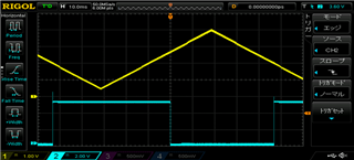
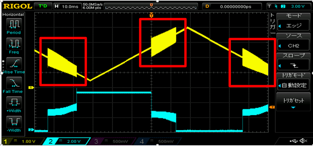
The data are shown below.

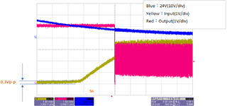
The output oscillates near the middle potential of VCC (approximately 2.5V) for a very slow rise of the input.
This is a common phenomenon in products without Schmitt triggers.

I don't know how to make sense of this anomalous phenomenon.
Could you please help me to find out the cause?

Best regards,

Higa

  • Hello Higa-san,

    Can we find out if the device has sufficient and well placed bypass capacitance? Schmitt-trigger inputs are very resiliant to slow signals, but if there is little or no bypass capacitance placed electrically close to the device, they can have similar oscillations to a standard CMOS input device.

  • Hi Maier-san

    Thank you for your reply.

    I confirmed that there are some bypass caps.

    Additional verification by the customer confirms the absence of hysteresis in the product after the process change. (Please attached excel file.)

    Please let me know if you have any question.

    Best regards,

    Higa

    1638.SN74HC14APWR  data of mesurement Vin vs Vout 2022_12_20.xlsx

  • The HC14 indeed should have hysteresis.

    Please show the marking of these devices? Is it HC14/HC14A or HC04/HC04A?

  • Hello Higa-san,

    I would recommend to verify that the parts are indeed HC14 and not HC04 (or any other device marking) as Clemens suggests.

    If they are indeed SN74HC14 devices, my next recommendation would be to verify that they came from an approved vendor.

    Assuming both of the above are true, then they should start a return through their vendor. When asked, they should indicate that the device is failing the hysteresis specification in the datasheet and provide the information in the Excel spreadsheet you have provided to us.

  • Hi Maier-san

    I attached marking photo of  these device as follow.

    This product is delivered from an authorized distributor in japan.

    Best regards,

    Higa

  • Hello Higa-san,

    It looks like you're using the Japan only variant - SN74HC14A, and not the standard SN74HC14. I would recommend to start a return with the supplier to determine why the device seems to contain the '04 function instead of the '14 function.

  • Hi Maier-san

    Thank you for your suggestion.Sorry to get back on topic, but there is something I would like to confirm with your previous comment below.
    Is it correct to understand that "bypass capacitance" is the capacitance that should be inserted between the VCC pin and the GND pin?
    Do you have any recommendations for proper capacitance and placement?


    ``but if there is little or no bypass capacitance placed electrically close to the device, they can have similar oscillations to a standard CMOS input device.''

    Best regards,

    Higa

  • Hello Higa-san,

    From the SN74HC14 datasheet:

  • Hi Maier-san

    Thank you for your kind support!

    As a result of further verification, we confirmed that there is a large change in input impedance (variation in input current?) near the threshold (Vt+ or Vt-).

    Therefore, we added capacitance(0.1uF connected to GND) at input, and both the input and output became stable.

    At the same time, we were able to confirm that there is hysteresis in input.

    The captured image of the oscilloscope is below.

    The left is without a capacitor on the input and the right is with a capacitor.

    In addition, the same phenomenon was observed when checking the sample before the process change with the same circuit and conditions.

    It seems that the input impedance variation has always existed, not due to process changes.

    Why is there such a large variation in input impedance?

    We had a hard time predicting this from the datasheet.

    Best regards,

    Higa

  • Hello Higa-san,

    Input impedance is only specified as a typical capacitance value and a maximum input leakage current. I have not seen a large change in impedance at the inputs -- can you explain how you have determined that the input has this large input impedance change?

  • Hi Maier-san

    Thank you for your prompt reply.

    From the waveform, it can be inferred that the current flows strongly in and out near the input threshold.
    I thought of this as a variation in input impedance.
    Also, since this phenomenon did not change even when the capacitance between Vcc and GND was changed, it was determined that it was not caused by the power supply.
    We believe that our guess is correct, as it was improved by inserting a capacitor (0.1uF) to GND at input.
    The input voltage changes very slowly. (The time axis is s/div.)

    Best regards,

    Higa

  • CMOS inputs always have a high impedance. This means that high currents cannot flow, but it also means that a small current can result in a large voltage change.

    The output oscillations are caused by the inductance, of the pins and the bond wires, which makes the I/O and VCC/GND voltages on the die differ from those at the pins; see section 2 of the bus-hold application report.

    These oscillations cause high switching currents, which will affect all pins due to parasitic capacitances inside the packages. It is likely that the input oscillations are just an effect of the output oscillations (but amplify it in return).

  • Hi Ladisch-san

    Thank you for your reply.

    However, I think your comment  is regarding the device without Schmitt trigger input.

    As you can see from the data I attached, the output oscillates at an intermediate potential (neither H level nor L level).

    Maier-san

    I think that the output oscillating at the intermediate potential like this is clearly abnormal for the device operation of the Schmitt trigger input.

    What do you think?

    Again, this phenomenon was observed regardless of process changes.

    I would appreciate your help in investigating what could be causing this phenomenon.

    Best regards,

    Higa

  • A device with Schmitt-trigger input should never oscillate (if it has a stable power supply).

    So either you have a wrong device, or the power supply is not stable. Can you show an oscilloscope trace of that supply (at the top of R112, and/or at IC19)?

  • Hi Ladisch-san

    I have confirmed the stability of the power supply.

    It has been confirmed that input and output oscillations stop when a capacitor is inserted between the input and GND.

    How can this be explained?

    Best regards,

    Higa

  • Hello Higa-san,

    It cannot with the provided information - there is more going on than what you have said.

    If the customer can confirm that the device is not meeting a datasheet specification (in this case, hysteresis), then a return should be started through their supplier so we can properly investigate the issue.