This thread has been locked.

If you have a related question, please click the "Ask a related question" button in the top right corner. The newly created question will be automatically linked to this question.

TXB0102: Output noise prevents high-speed translation

Part Number: TXB0102
Other Parts Discussed in Thread: MSP430FR2433

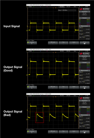
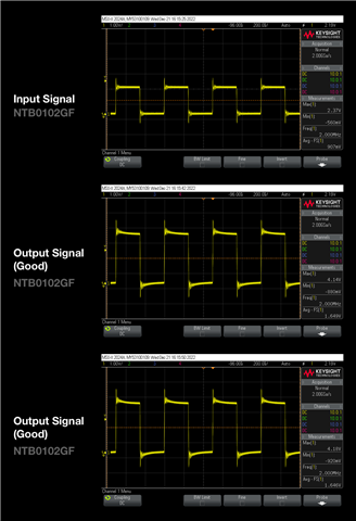
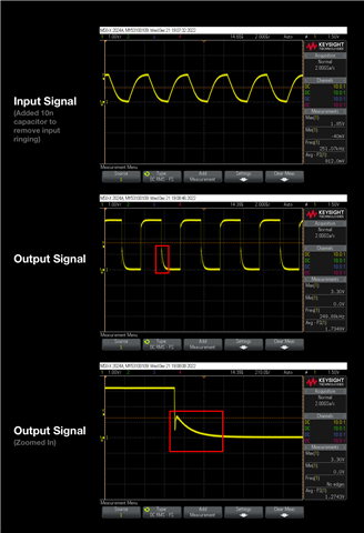
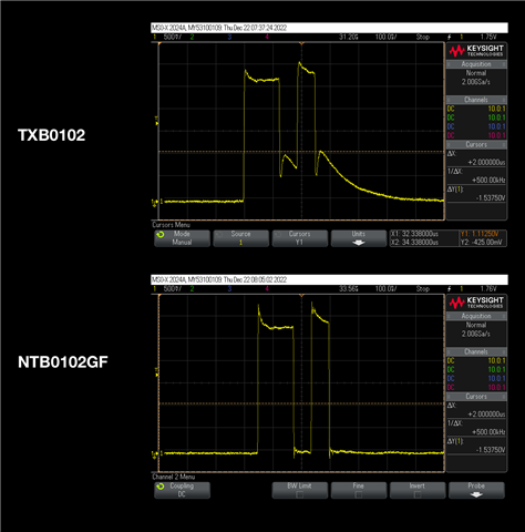
I'm using the TXB0102 and seeing noise that prevents using it above ~1MHz, but the datasheet claims 60 MHz (60 Mbps) for my VDD setup.

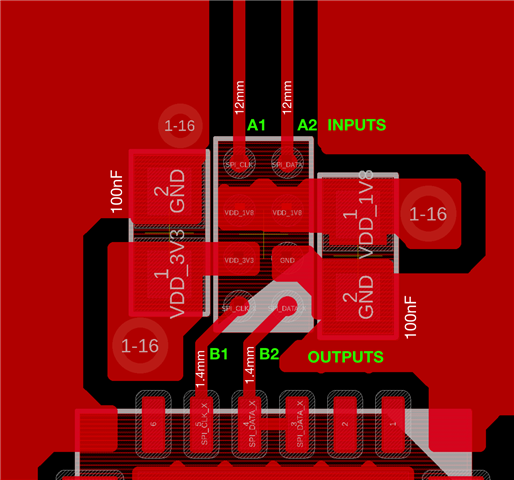
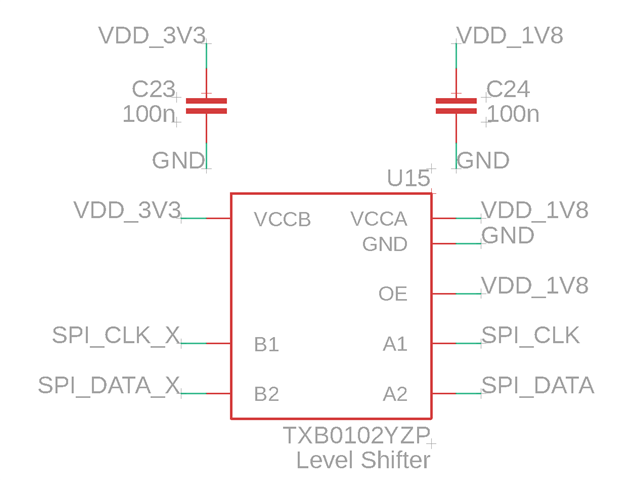
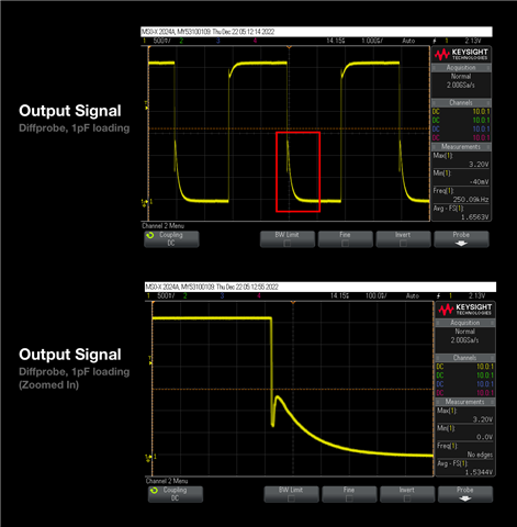
In the attached scopeshots, a 2MHz square wave drives TXB0102's inputs (A1 and A2). TXB0102's outputs (B1 and B2) are connected to separate pins of an MSP430. The MSP430 configures these two pins as digital inputs (no pullup/pulldown). Trace length is <2mm from TXB0102 output to MSP430 inputs, so pin+trace load capacitance is <15pF.

As the scopeshots show, one of the TXB0102's outputs behaves normally, while the other sees a spike and never settles to 0V, which prevents using it above ~1MHz.

Any idea what's going on here?

  • Further information: I replaced the TXB0102 with a new one and the problem persists, so the issue isn't a broken TXB0102.

    I also tried the same test on a nearly identical board, but with NTB0102GF instead of TXB0102, and the problem is fixed:


  • There is lots of ringing on these signals. I do not know how much of that is a measurement artifact, but it would be possible that ringing at the input causes the wrong edge accelerator at the output to trigger. Please try to properly terminate the input trace.

  • Thanks Clemens. To remove the input ringing, I slowed down the input signal to 250kHz and added a 10n capacitor to the input. (I know TXB0102 can't drive large caps, but in this test the cap is exclusively on the input side and TXB0102 isn't driving it, so I assume that's OK.) To remove the output ringing I added a 100 ohm series output resistor.

    The problem is still apparent with those changes:

  • Hi Dave,

    Could help provide the schematics? 

    As the scopeshots show, one of the TXB0102's outputs behaves normally, while the other sees a spike and never settles to 0V, which prevents using it above ~1MHz.

    Note that 60Mbps would mean 30MHz. Also, is the pin farthest away from the supply the concerning output? Are you using sufficient bypass caps as close to the supplies as possible? Do you have any delay circuitry (RC circuitry) with the TXB? Thanks.

    Best Regards,

    Michael.

  • Thanks Michael. Didn't realize 60 Mbps was for all pins, but 30 MHz is fine for me. Please see the attached layout for the board that exhibits the problem. Note the bypass caps for both supplies. No delay circuitry.

    An important detail that I glossed over previously: the broken output is connected to 2x MSP430 pins, while the working output is only connected to 1x MSP430 pin. All MSP430 pins are configured as digital inputs, and per the MSP430 datasheet (MSP430FR2433), each pin should have 5pF capacitance (hence my previous claim "pin+trace load capacitance is <15pF").

    I cut the B2 trace and measured the unloaded TXB0102 output, and the problem disappeared. So it seems the TXB0102 can't handle the load of 2x MSP430 pins. I'm at a loss to explain that, given the TXB0102 datasheet's "LOAD CIRCUIT FOR MAX DATA RATE" shows a 15pF capacitor.

  • Hi Dave,

    Thanks for clarifying. In addition to the layout, do you also have full schematics showing the TXB connected to the host?

    15pF should be of no concern. However, do you have connectors with B2 and the 2x MSP430 pins; as they also add additional capacitance? Thanks.

    Best Regards,

    Michael.

  • Thanks Michael. Schematic attached but it's probably not too helpful. The full schematic is large and I can't share much of it, but in summary there's a chip driving A1/A2 from GPIOs via 12mm traces and nothing else on the lines. Do you need more than that, given the provided input signal waveforms?

    There are no connectors connected to B2 other than the oscilloscope probe. I just measured with a differential probe to lessen the loading (probe specs say 1pF loading). Problem persists, see attached.

  • Here's one last motivating example comparing TXB0102 and NTB0102GF. Nearly identical boards but different level shifters. In both cases, the MSP430 receives the same data from the slave at the desired 16 MHz. Measured with the 1pF diffprobe.

  • Hi Dave,

    I understand, as the full schematic would have further helped.

    However, it is unusual that the NTB part isn't seeing a similar issue with the same host and drive strength. Do they both have a similar layout for similar spacings?

    Best Regards,

    Michael.

  • The layout is nearly identical. I just measured the difference between trace lengths between the boards; the delta for the A1/A2 traces is 0.7mm, and the delta for the B1/B2 traces is 0.32mm.

    Thanks Michael. Hope you're not working too hard over the holidays :)

  • Hi Dave,

    I am happy to help :).

    By nearly identical, could you help clarify any differences? Is the delta for the NTB case similar?

    Is the observation significant enough to change the states of the device? Could the traces be moved significantly further apart while observing the impact? If not feasible at all, could you try using a low-pass filter while observing the impact? thanks.

    Best Regards,

    Michael.