This thread has been locked.

If you have a related question, please click the "Ask a related question" button in the top right corner. The newly created question will be automatically linked to this question.

SN74LVC1G17: 'Peak' inrush current

Part Number: SN74LVC1G17
Other Parts Discussed in Thread: SN74HCS244

Hi Team, 

Good day. I am posting this inquiry on behalf of our customer. 

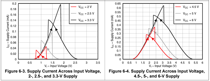
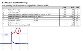
We are currently designing a new product in our microwave/steam oven product range and we are looking at part No. SN74LVC1G17, which we use in other products, as a good component to meet the requirements. What I cannot find in the standard specification, is the 'Peak' inrush current, these components are rated to.

Please could you let me know what this ‘Peak Inrush Current’ is and send me further details/specifications to verify this?

Please help to advise. Thank you for extending your support.

Kind regards, 

Marvin

  • Hi Marving,

    The peak inrush current should be the "Continuous current through VCC and GND" spec in our datasheet. This is the input current + the output current. Let me know if this is not what you are looking for. 

  • Hi Albert,

    Good day.

    The customer is asking for more detailed specifications for this device. What they would like to know is what the ‘Surge’ current for this device ie. The instantaneous current when initially powered up etc.

    Please advise.

    Regards,

    Josel

  • Hi Josel,

    There is no 'surge' current for starting up a CMOS logic gate, thus it is not a specification for any CMOS logic gate. There is inrush current for the supply capacitor.

    The bypass capacitor that is required to be connected to the supply and ground pins of the device will draw a significant current at startup, usually calculated with the power supply ramp rate and capacitor size.

    From the application report here: https://www.ti.com/lit/pdf/slva670

    dV/dt can be changed to a discrete value assuming the supply ramp is linear, using V_final / t_rise

    For an example, if the customer uses the recommended 0.1uF capacitor for the supply and has a supply ramp rate of 1V/us, then the current required is 0.1uF*1V/us = 0.1A = 100mA. We expect that the ESR of the capacitor is small, so it is likely that the current would be close to this value, and the time to charge the capacitor to 5V would be 5us.

    -

    A CMOS device also has shoot-through current caused by both the N and P FETs being on at the same time when switching states at the input. As long as the input transition is fast, this will be for a very short time and generally will be negligible (the instantaneous current is drawn from the bypass capacitor, and the average current is extremely low).

    Since this is a Schmitt-trigger input architecture device, the input transition can be much slower, and the device will draw additional current during this time.  The datasheet provides one data point, referred to as dIcc:

    This is only valid when the input is at V_cc - 0.6V. The current will increase more as the input move away from the rail. The maximum value is not specified.

    I would expect the maximum value to be in the range of several milliamps. If you need a device that shows the full range of current, please take a look a the HCS logic family - for example, the SN74HCS244, which has this plot showing the typical supply current due to input voltage:

  • Hi Emrys,

    Good day.

    Thanks for getting back to me. That verifies a couple of things for me. There is an additional parameter I would like to know.

    Could you confirm the ‘peak’ output current ( Drive Current) it can sink / supply? The specification specifies a constant of 50mA. Is this also the peak current or is there an instantaneous current it can sink / supply? Just considering the effect of ‘smoothing’ capacitors we have on the output line etc, to other components.

    Hence, do we need to restrict this instantaneous output current demand, from this device when switching low (driving low)?

    Regards,

    Josel

  • The absolute maximum rating of 50 mA is a limit that your circuit must avoid in order to prevent damage. If you short the output to GND or VCC, the actual current can become much larger, more than 150 mA.

  • Hi Clemens,

    Just to further clarify what I need to know:- 

    The SN74LVC1G17 is specified as having a maximum Continuous Output current of +/-50mA (see below).  Please advise if  there a Peak Output Current Limit, for example, if point A is 200mA for a brief period. Is this acceptable, provided the ‘average’ is within +/-50mA.  For what duration could a Peak current of 200mA be sustained without affecting the operation or lifetime of the part? A typical plot is shown below.

    Regards,

    Josel


  • There is no separate peak current limit. The specified limit applies even to short periods.

    (Actually, capacitive loads of up to 70 pF are allowed.)