SOM CARD_20230217_LA.pdfSN74LVC1G373 SCH review
This thread has been locked.
If you have a related question, please click the "Ask a related question" button in the top right corner. The newly created question will be automatically linked to this question.
This part of the schematic does not show a decoupling capacitor.
With D connected to GND, the output can never be high, so RESET_D never has an effect. Only PMIC_EXT_EN_OUT_R switches the output between GND and Hi-Z.
What is the purpose of this circuit? What effect should RESET_L have?
Hi Leo,
May I know which pin needs a decoupling capacitor., is VCC pin?
Yes, VCC for any logic device should have a 0.1uF bypass capacitor. From the datasheet:
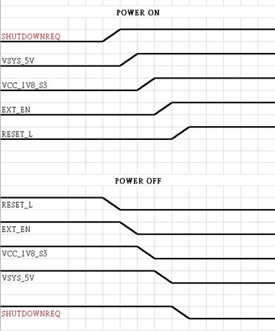
When power on, EXT_EN will be high, output will be high Z mode,
When power off, RESET will be low, and EXT_EN will low, out put will be low to shutdown my carrier board power
I'm not sure this circuit will do what you expect. The Q output at power up (VCC_1V8_S3 turn on) is unknown - the latch does not have a known output state until it has been loaded with data.
The signal RESET_D could only have an effect if Q happened to start in the high state, after which it would no longer have an effect as the latch would remain in the low state.
The pull-up to VCC5V0_SYS will cause the output to go to 5V when Q is in the high-impedance state, however this won't set the latch state to high - as soon as the output is enabled again, it will be pulled back to 0V.
When system power on, we want shutdownreq keep high, shutdownreq was link to our carrier board 5V EN pin.
When system power off, we want shutdownreq after EXT_EN change to low, shutdownreq output change to low state, to turn off 5V EN pin.
EXT_EN this pin can show our PMIC IC state, EXT_EN high was system turn on, EXT_EN low was system turn off
The Q output at power up (VCC_1V8_S3 turn on) is unknown -> my output has a PU RES, I think it will keep high, we expet only system turn off, this circuit will be active, and when EXT_EN change to low, output Q also change to low to shutdown my carrier board power en pin
The initial state of the latch is undefined; see [FAQ] What is the default output of a latched device? (Flip-Flop, latch, register) If the initial state of the latch happens to be low, then it will actively drive its output low, and the pull-up resistor will have no effect.
The latch is powered by VCC_1V8_S3, so its output can go high only when VCC_1V8_S3 is powering up, and must go down when VCC_1V8_S3 is powering down. But the pull-up resistor to VCC5V0_SYS means that the output will be pulled high when the latch is powered down, so the SHUTDOWN_REQN_5V signal will go up and down when VCC5V0_SYS is powering up/down.
Is VSYS_5V the same as VCC5V0_SYS?
In your timing diagram, you have shown all edges at different times. But this is not possible; the SHUTDOWN_REQN_5V can change only when (at least) one of its inputs change, or when its power supply changes. Please specify exactly how the value of SHUTDOWN_REQN_5V is determined by the other four signals/supplies.