This thread has been locked.

If you have a related question, please click the "Ask a related question" button in the top right corner. The newly created question will be automatically linked to this question.

SN74HC373: internal protection for input /output

Part Number: SN74HC373

Hi team,

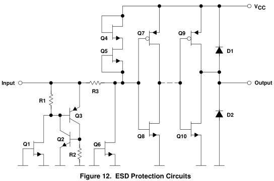
My customer wants to confirm the internal input or output protection for these deivces. Protection like the clamping diode.

• SN74HC373APWR
• SN74ACT373NSR
• SN74LV373APWR
• SN74HCT373NSR

Could you kindly share us the internal circuit for this?

Regards,

Ohashi

  • The presence (AC, HC) or absence (AHC, LVC, LV-A) of a positive clamp diode can be derived from the datasheet; see [FAQ] Can the input voltage (Vi) to my logic device be higher than the supply voltage (Vcc)?

    The details of the internal circuit are secret, except for AHC (see section 2.3.1 of the AHC Designer's Guide):

    Figure 12 shows protective circuits used for advanced high-speed CMOS devices. To meet the requirements outlined previously, the protective circuit is constructed in two stages. The input is first protected by a thyristor consisting of transistors Q2 and Q3. This provides coarse protection. If the input voltage rises above about 15 V, transistor Q1 breaks down and fires the thyristor. The latter then short circuits the high currents. Resistors R1 and R2 have values of only a few ohms. Therefore, the holding current of the thyristor is several tens of mA. When the current is reduced again at the end of the discharge, the thyristor is extinguished. Transistors Q4, Q5, and Q6 operate as fine protection and are intended principally to protect the input from excessive voltages. When there are overvoltages at the input, these transistors are driven into breakdown and limit the voltage, while resistor R3 limits the current.