This thread has been locked.

If you have a related question, please click the "Ask a related question" button in the top right corner. The newly created question will be automatically linked to this question.

SN74V293: FIFO data out isn't always the FIFO data that went in.

Part Number: SN74V293

I have an application where a 74V293 is connected between a microcontroller and a parallel DAC to provide an "elastic" buffer between the two, and to enable the data to the DAC to be transferred at a well-controlled rate.

I've tried with a few variants of the 74V293, including the EP version, and the -6 and -7 standard product speed grades.

Most of the time it works fine but, in this application, about once in every 200 times the data coming out of the FIFO isn't the same as the data going in.

There are no obvious causes.  For example, I monitor the full and empty flags, and they're never asserted.  All aspects of operation look the same both when the output is as expected, and when it isn't.

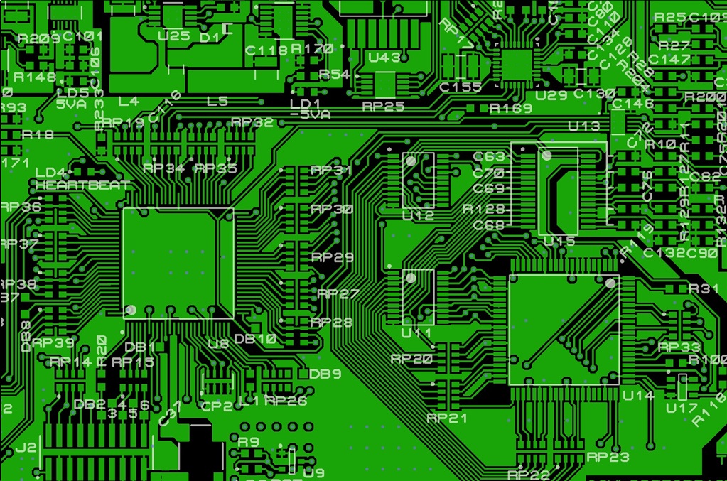
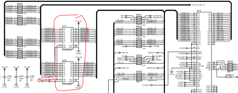
The schematic is shown in this thread: https://e2e.ti.com/support/logic-group/logic/f/logic-forum/874433/sn74v293-unexpected-offset-value

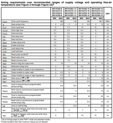
Only D0-D15 and Q0-Q15 are used, since the output drives a 16 bit DAC.  The FIFO is configured to operate as a 65536x18 memory.

Data is written to the FIFO in bursts of 8192 values.  Readout is at a constant 25MHz.  The data written is cached by the microcontroller, so is written at an average rate of about 30M values/s, but is actually written in even shorter bursts that are several cycles in length, and have an even shorter cycle time.

I have, though, tried extending the data setup time so that the write cycles have very conservative timing.  That doesn't eliminate the problem.

The programmable empty flag operates sycnhronously, is set to 49152, and is used to trigger a FIFO refill. 

I'm limited to a 16 digital + 2 analogue channel MSO for debugging, so I can't easily monitor the input and the output.  If I operate this particular MSO so it records a clocked parallel bus, I'm limited to monitoring the enable and clock lines with 14 bits of the data bus.

But, by monitoring the input and output separately, I can see that the data being written to the FIFO is always correct, but that what emerges on the output is sometimes corrupt.

Normally, the data represents a sinusoidal signal.  To try and get more of a handle on what's happening, I've tweaked the code so that when this problem occurs, the data written is a linear sequence from 0 to 65535, with an increment of 2 (for reasons of convenience that I won't bother with here).

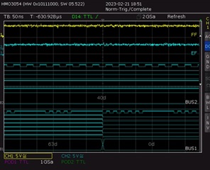
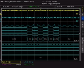
It immediately becomes clear what is happening at the output when this linear test sequence is monitored:

(Not sure why the image quality has deteriorated so much when uploaded, but I think it's clear enough to follow).

The top yellow trace is the DAC output: ignore that.  The blue traces are, from the top, REN, RCLK, Q2-Q15.

It's clear that whenever an output bit transitions from low to high, all the lower order bits, as far as and including Q5, then toggle for the next 8 RCLK cycles.

For legibility the screenshot only shows a selection of bit transitions.  But the phenomenon occurs at all low to high transitions of Q5-Q15, including the non-existent transition of Q16.

I don't think the glitches on REN are "real".  I think they're an artifact of the less-than-ideal probing, which involves a lot of skinny bits of wire making the board into an electrical porcupine.

What is causing the unexpected data pattern?

I've been probing around the circuit and trying different tests for days, and can't come up with any mechanism that could cause this to happen.

Any suggestions would be appreciated.

Colin

  • Hey Colin,

    I don't have much experience with our memory ICs... The person who can help you is out today (2/21), but should be in tomorrow Wednesday (2/22). I will forward this request to him and hopefully he can help you out more. 

  • Hi Albert,

    Has your colleague had a chance to take a look at this problem?  I'm no closer to finding an explanation or a solution.

    Regards,

    Colin

  • Hi Colin,

    Most of the time it works fine but, in this application, about once in every 200 times the data coming out of the FIFO isn't the same as the data going in.

    Based on this description, my expectation is that there are times when the timing requirements may not be met, which could result in incorrect data being stored.

    The first things I would recommend looking at are the analog input waveforms -- the above digital analysis is helpful for checking the data, but it is possible for the logic analyzer to identify one value/timing while the device itself does not necessarily 'see' the same value. There are quite a few timing constraints in the datasheet:

  • Hi Emrys,

    Thanks for the reply.  From the outset the design has used conservative timing.

    I understand your point that the logic analyser and FIFO may have different logic thresholds, but I've inspected the waveforms using analogue channels, and the rise and fall times are fast enough to ensure the timing constraints are easily met.

    This is a screenshot from the scope simultaneously showing the upper 6 bits of the both the input and output buses, with a high-to-low transition on all bits on the input bus ('D' bus):

    This is a screenshot with a high-to-low transition on all the output bits ('Q' bus):

    The EF and FF flags are on the analogue channels.  They should never be active, and I don't see any activity on them, even when the output data is incorrect.

    The output is clocked from the FIFO using a fixed 25MHz clock source.  REN is fixed low.  I don't think there's much that could go wrong on that side.

    On the input side data is transferred using the static memory port on a STM32F4 microcontroller.  You can see from the screenshots that write pulses are about 11ns wide.  It's not so clear from the screenshots, but data is stable at around the falling edge of WCLK, and remains stable until the next write cycle, so the data setup and hold times are easily met.

    WEN is held low for the duration of operation.

    The two screen captures are at different times since there's a delay of 2.6ms between data being written to the FIFO and then read out from it.

    Given that the read and write clocks are much slower than the specifications require, and the data setup and hold timing requirements are met, what other timing violations could cause this issue, where the output data permanently ceases to match the input data?

    Colin

  • Hey Colin,

    (Not sure why the image quality has deteriorated so much when uploaded, but I think it's clear enough to follow).

    For E2E posts, when you attach an image, you can select the image in your post and then select the 'edit' button on the bottom left. In that popup, you can then change the display resolution (I usually just set the width to 800 and leave the height blank to keep the aspect ratio). I'm sure it was done to save memory on the server, but it is quite a frustrating 'feature' of E2E.

    -

    My first check would be to look at the analog input / output signals when the issue occurs. It looks like the DAC goes a bit crazy when the error occurs, so you could use that as a trigger to see what's going on... I'm not sure how deep of a memory scope you'd need to catch over 2.6ms of history at a nanosecond scale though.

    To be frank, I don't look at these devices very often - in fact, I can't remember a single question on them in the last 8 years I've been supporting logic for TI. I'm going to reach out to another TIer to see if they might have some helpful input.

  • Hi Emrys,

    Point noted about the embedded images.

    The link I included earlier in the thread was to a question I asked about these devices a few years ago.  I developed a workaround to the bug I found back then.

    This problem was first spotted as a result of the output waveform from the DAC being wrong, but it's a difficult "wrong" to trigger on!  That's why I've been probling the FIFO's control and data signals, and trying to trigger on the activity there.

    The scope I have can capture 4Mpts, so I can get a few ms of data.  The challenge is finding the few ms of data that illuminates the problem.

    Thanks for the ongoing help.

  • Hey Colin,

    While I'm waiting to hear back from my colleague, I can give you a couple things to look at.

    I found an older post from you on a similar topic -- is this a relatively new issue for you, or a gremlin you've been chasing for a while?

    Assuming it's been going on a while, I'd like to look at less likely solutions / things that probably wouldn't have been looked at yet.

    Layout issues can result in cross-talk and reflections that might cause incorrect values to be either written or read out from a device. Is it possible for you to share the board layout?

    If you can't share, I'd recommend you to review the ground plane / power planes in the board and verify that they aren't significantly cut near the channels in question affecting the impedance and crosstalk of the signals. At least on the BGA, these pins are very near each other:

    It may also help to observe the wire delays on the input side from your test points -- it's probably not an issue, but it can't hurt to see if anything is significantly different that might cause the timings to be closer than expected.

  • Hi Emrys,

    A colleague of mine found this issue a while ago, but hadn't reported it to me until recently.  Because it was an intermittent and occasional issue that wasn't causing serious problems they'd put it to one side.

    The older post you mention is the one I linked to because it includes the relevant section of the schematic, to save uploading it again.  The older post was a different issue, but does relate to these parts.

    On this board I use the QFP package.

    The board is 4-layer, with local ground and power planes and double-sided assembly.  The following images (better resolution this time!) are the area around the processor and FIFO, in order of top copper, ground plane, power plane, bottom copper (I'm not going to put the manufacturing files onto a public forum, but the images should give a good idea of the layout: there aren't any cuts in either the ground or power planes under the processor and FIFO).

    I've kept the top side legend on all but the bottom copper so they're easy to align.  On the bottom copper I've used the bottom side legend since there are components there (the bottom side is mostly used for decoupling capacitors, of which there are many).

    The issues affect all the data lines.  The total trace length of each of the data lines does vary, from a minimum of about 35mm to a maximum of about 70mm.  The write clock trace length is about 95mm.

    I wouldn't expect those differences to create a difference in edge timing of more than a few hundred ps, and that's being pessimistic.  Given the setup and data time requirements, even a small number of ns of timing difference shouldn't cause a problem.  And, as I noted, the problem persists if I extend the data setup time in the microcontroller external bus configuration.

    observe the wire delays on the input side from your test points

    I assume you're suggesting I see how much spread there is of transitions at the test points.  At the limit of the resolution of the scope I have (2GS/s), I don't see any variation.  The equipment I have here isn't capable of taking measurements any more sophisticated than that.

  • Hey Colin,

    Your layout looks good to me - it was a bit of a long shot idea.

    I discussed with someone who supported these devices closer to the time they released, and he said that the two issues he saw most commonly were the power up timing sequence, and the reset signal sequence. Apparently if those aren't followed precisely, the device can end up in an incorrect state that might cause issues. I don't think that's the issue you're having, but it's at least worth a look.

    I've also asked another member of my team who is experienced with similar systems to take a look at this issue to see if anything pops out to him.

  • Hi Emrys,

    I don't think it could be a power up sequence because the mismatched input and output data occurs without power being cycled.

    But the device is subject to a complete master reset sequence frequently.  As you might expect, the DAC that connects to the FIFO output is used to generate a waveform.  Every time this unit has the output waveform changed, the FIFO is re-initialised, re-tested (there's lots of defensive code), and then the new output is generated.

    The master reset sequence shown in the datasheet doesn't look complex.  On each re-initialisation the pins used to configure the device are set to the appropriate levels, and the master reset is pulsed.  I've implemented very conservative timing: the master reset pulse is active (low) for about 1us.

    After the master reset is complete, the programmable flag offsets are programmed using the parallel interface (only the programmable partially empty flag - PAE - is actually used in the application).

    Given the bug I discovered a few years ago (the link is earlier in the thread), reading back the programmable offsets through the parallel interface doesn't return the correct values, so the software proceeds to completely fill the FIFO with known values, then drains it until PAE goes active to verify the correct value has been loaded.  Each value clocked out of the FIFO is also verified, so the FIFO effectively undergoes a full self-test each time a new output is configured.

    In this application the fractions of a second that that all takes aren't noticeable.  Much the same happens with other components in the system.

    The FIFO is then completely filled with waveform data, and the read clock is enabled.

    As the FIFO drains, PAE becomes active, and new data is transferred in to continuously produce the output from the DAC.

    If the self test part of the process doesn't return the correct values for offset and data transfers, an error is reported, but I don't ever see that happen.

    Can you spot anything I might I have overlooked in the sequence?  Or where might timing in that sequence be sufficicently critical that timing errors might cause the device to end up in a state that could cause issues?

  • Hey Colin,

    Would it be possible for you to force a disable condition on these two buffers and see if the issue continues to exist? My colleague here suggested that there's no protection for bus contention between this device and the DAC or FIFO, so it may be an intermittent issue there.

  • Hi Emrys,

    The buffers are disabled when the output signal is being generated.  It would be complete chaos on the output if they weren't!

    It's easy to miss signals on the schematic, though: the buffer disable signal is highlighted here:

  • Hey Colin,

    Emrys is currently out of the office today. He should be back tomorrow and can keep supporting you on this.

  • I'm afraid I'm out of ideas.

  • Hi Emrys,

    Thanks for the support and ideas.  When I get to the bottom of the issue I'll post an update.