This thread has been locked.

If you have a related question, please click the "Ask a related question" button in the top right corner. The newly created question will be automatically linked to this question.

SN74LVC1G04: Data retention logic levels

Part Number: SN74LVC1G04
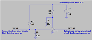
Other Parts Discussed in Thread: SN74AUP1G04, SN74AUC1G04, , SN74LVC1G240

The datasheet specifies "data retention only" down to 1.5V. Our understanding is that this means that the circuit will hold the output at the same level if the supply drops into the 1.5V to 1.65V range.

1) However, is there also an expected behavior when considering ramping up into the 1.5V to 1.65V range?

If the input (A) is kept at (or slightly higher than) the the supply voltage when ramping up the voltage, then...

2) what is the expected behavior when passing 1.5V?
3) what is the expected behavior when passing 1.65V?

Is it for instance undefined, or should we perhaps assume that that the output goes high even if the input is as high as the supply? 

  • "Data retention only" means that the device works correctly as long as it does not need to react to any input changing or need to switch any output. When starting up, it is possible that the internal state is not the same as that demanded by the input signal, so in this case, there is no guarantee that the output is in the correct state.

    You need at least 1.65 V for the device to start working correctly. Later, supply voltage dips down to 1.5 V can be tolerated as long as the inputs do not change.

    For low-voltage applications, devices like the SN74AUC1G04/SN74AUP1G04 usually are a better idea.

  • Thank you for feedback!

    Does this mean then that when ramping the supply for the SN74LVC1G04 (for instance from 0V to 3V), there is no way to ensure that the output stays low during the complete ramp? I assume that during a monotonic ramp-up, once we reach Vcc = 1.65V it is enough to keep the input pin above 0.65xVcc (or 1.7V), but before we reach 1.65V it does not matter what the input pin voltage is, the output might go high even if the input pin is held high all the time. Correctly understood?

    This is a critical detail for our design. We need an inverter that drives the output high (to Vcc) ONLY when the input is low relative to Vcc, including during Vcc ramp-up. The input pin can be assumed to ramp faster than the Vcc pin (same supply, but using RC circuit).

    Would you have any alternative part number to propose? It must be able to handle up to Vcc=5.5V. The input pin will maximum go to the same voltage as Vcc.

  • Below I add an example circuit to further clarify the setup we aim to achieve.

    Example circuit

  • The power-up behaviour is not guaranteed. But devices with /OE (e.g., SN74LVC1G240) can be disabled during power up.

  • Something like SN74LVC1G240 sounds like great advice.

    In the datasheet I read "To ensure the high-impedance state during power up or power down, OE should be tied to VCC through a pullup resistor". Is it correct to understand then that /OE will be considered high (output high-Z) just by following Vcc, all the time when ramping up Vcc from 0V? For instance, when Vcc reaches 1.5V, will it keep the output high-Z if /OE is only 1.5V as well?

  • it correct to understand then that /OE will be considered high (output high-Z) just by following Vcc, all the time when ramping up Vcc from 0V?

    Yes, that is correct.

  • Great! Then it seems we are almost there. I just want to ensure we understand this part correctly as well: "the minimum value of the resistor is determined by the current-sinking capability of the driver".

    I assumed the /OE pin is a high impedance digital input, not really sinking any current. What I see in the datasheet is a max of 5 uA. Is that sentence referring to that we should not pick a too high resistor value (stay below 10 kOhm or so) so that we get a voltage drop from those max 5 uA? 

    I sort of assume I misunderstand since it says minimum, not maximum. What is then the sinking capability to consider?

  • What I see in the datasheet is a max of 5 uA. Is that sentence referring to that we should not pick a too high resistor value (stay below 10 kOhm or so) so that we get a voltage drop from those max 5 uA?

    It is important to avoid too large of a resistor for this reason, but it's not the meaning of that particular sentence.

    the minimum value of the resistor is determined by the current-sinking capability of the driver

    The driver in that sentence is the signal source - ie the device driving the digital signal to the OE\ input. We assume you must be changing that OE\ state with some kind of signal driver once the system starts operating - otherwise the device would never output a signal with a pull-up resistor on OE\.

    If, for example, your signal source can only provide V_OL of 0.5V at I_OH = 100uA, then the pull-up resistor would also have to be relatively large to allow the driver to change the input state correctly.