This thread has been locked.

If you have a related question, please click the "Ask a related question" button in the top right corner. The newly created question will be automatically linked to this question.

SN74AUP1G14: Sine wave (or clipped) to square wave for FPGA clock

Part Number: SN74AUP1G14
Other Parts Discussed in Thread: SN74AHC1GU04, SN74LVC1GX04

Hi to all users.
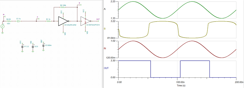
I need to design 3.3V FPGA board with clock from TCXO.
TXCO would give me sine wave or clipped sine wave.
TCXO I am actually using is 32MHz (I need 48MHz but it should work up to 100MHz), outputs levels of clipped sine wave are 0.12 to 1.04V.
I would like to use low pin count inverter (such SN74AUP1G14DBVR in SOT-3 package).
Unfortunately there is no availability of TCXO from my supplier, so I am not sure which oscillator I'm going to use (just powered 3-3.3 Volt) and I have no way to create small PCBs for test.
Is there a reference circuit I can use as general purpose to convert sine (clipped) to square wave?
Thanks.

  • Hi Michele,

    The device you have selected, SN74AUP1G14, is a logic inverting buffer that will provide a square wave output, but only with the appropriate input levels.

    There are a few different ways to approach your solution, but my recommendation would be to use an unbuffered inverter to convert your sine wave to a square wave, likely with a slow slew rate, and then send that signal into the SN74AUP1G14 to convert to a clean sine wave.

    The above is a simulated version of what I described. You can see how the small input voltage (IN) is converted to a kind of square wave by the first inverter (from A to B), then the Schmitt-trigger inverter changes that to a clean square wave output.

    Using this approach, you may not have a precise 50% duty cycle, but you should get consistent results and the appropriate frequency at the output.

    My recommendation for the two inverters would be:

    SN74AHC1GU04 - unbuffered inverter

    SN74AUP1G14 - Schmitt-trigger inverter

  • I forgot to include my simulation file:

    Sine-toSquare-wave-converter.TSC

    The real trick to this circuit is converting the sine wave to the appropriate bias voltage, which is handled by self-biasing the unbuffered inverter via the feedback resistor.

  • How fast!
    Thanks for reply.
    Due you use both unbuffered and buffered, could I use in the same way (browsing in the TI website I've found this) ST74LVC1GX04?

  • Due you use both unbuffered and buffered, could I use in the same way

    I would recommend against using a buffered inverter for the first stage - while it _can_ work, the parts aren't really designed for that type of application, so you might run into instability.

    (browsing in the TI website I've found this) ST74LVC1GX04?

    Yes - the SN74LVC1GX04 technically includes 4 unbuffered inverters, 3 of which make a buffered inverter, in the same package for specifically this type of application. Since they are all built on the same die, the transistors are matching and you're not going to get any issues from the slow input signal coming out of the first stage.

    This is a very common method for driving a crystal to produce a clock signal. We're just replacing the crystal with your sine wave source.

  • Little misunderstanding, when I say "unbuffered and buffered at the same way" I mean unbuffered + buffered of your schematic using unbuffered +buffered parts of ST74LVC1GX04.

  • I expected that was the case, but I wanted to clarify in my answer. I think you correctly understand this application.