A related question is a question created from another question. When the related question is created, it will be automatically linked to the original question.
If you have a related question, please click the "Ask a related question" button in the top right corner. The newly created question will be automatically linked to this question.
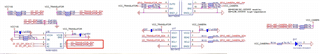
The TXS has open-drain outputs; the high output voltage is generated by the internal 10 kΩ pull-up resistors. These are not strong enough to complete override the 10 kΩ pull-down in the CTL input.
Use a buffered, unidirectional translator like the TXU0102.
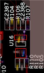
when i move away the U16,and test PIN 4,5。the signal is fine。then i think it is not the input signal problem。it may be the ISO1541 problem,its min input current is 3.5ma.what do you think?
The TXS is optimized for fast signals, but for I²C, you could just as well use a translator without edge accelerators, such as the LSF0102. But there is no P2P device.
The TXS is not a buffered device but a passive switch. If you want an output current of 3.5 mA, the device on the other side must be able to sink 3.5 mA.
And the ISO1541 does not require 3.5 mA; it supports output currents up to 3.5 mA.
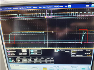
What you are experiencing is due to false triggering of the TXS one-shots.
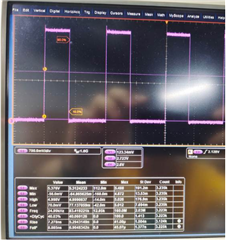
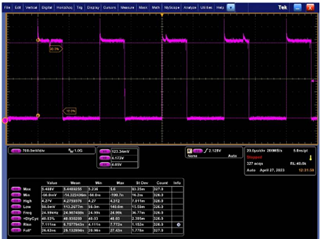
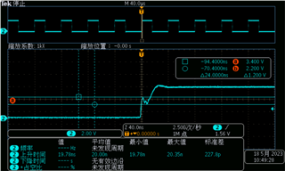
Note that the one-shots are designed to trigger when they detect rising or falling edges. As you can see, reflections / ringing can cause false triggers.
Similar to Clemens' feedback; ringing is also caused by capacitance and inductance of long cables / traces and can also be amplified by unstable GND or VCC voltages.
When you disconnect the ISO device, you are reducing the the lumped capacitance. Hence, you do not see the issue.
If it is not feasible for you to keep the traces minimal similar to section 11.1 of the datasheet, the recommendation would be the TXU0102 for U124 and the LSF0102 for U16 where you don't have one-shots to amplify your ringing, while also having the flexibility to include pull-ups to increase drive strength for signal integrity, thanks.
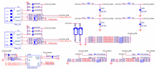
hello,this is our layout,i do not found problem。and Do you mean that in addition to replacing the chip, you can also try to reduce the pull-up resistor to try to solve the problem?
Your trace is very long. Note that this will add parasitic capacitance in addition to any load capacitance used.
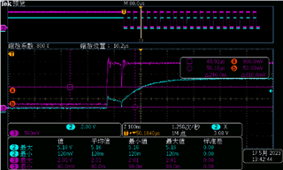
Also, is blue the input? The rise time is very slow. Are you meeting the datasheet's input transition rate for 10ns/V max? This is also impacted by the lumped capacitance if >70pF total.
Do you notice the signal improving when the frequency is reducing to the lowest you can go?