This thread has been locked.

If you have a related question, please click the "Ask a related question" button in the top right corner. The newly created question will be automatically linked to this question.

SN74GTL2003: How do the NMOS transistors work when the high side (Dn) is high?

Part Number: SN74GTL2003

Hello,

I am wondering how the internal transistor in GTL2003 will work under the following condition. 

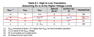
I have already checked Table 8-2 in the datasheet that the output state of that transistor will be VTT and the transistor will be ON. But I don't understand what the transistor does to make Sn go to Vtt level. Could you explain the behavior of the transistor in DETAIL?

Question

1. Could you explain the mechanism by which the transistor turns on under the following conditions?

2. There is no voltage source (pull-up resistor) on the output port (Sn) side. How does the output port (Sn) make the VTT voltage level when the input port (Dn) side is high?

3. If the device connected to the Dn side uses a push-pull port, is it not necessary to use a pull-up resistor on the Dn side?


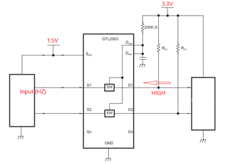
No pull up resistor on the Sn side.


Thanks.

  • Hi Seung-Gon,

    Could you explain the behavior of the transistor in DETAIL?

    Note that the GTL device is similar to LSF. Hence, please help see Understanding the LSF family of bidirectional, multi-voltage level translators further clarifying the behavior of the transistor in great detail showing how all the FETs are tied together (including Sn). With Dref and Gref externally shorted, this provides the gate voltage for all the FETs of the device. With the difference between Gref and Sref ≥1.5V, large enough for the FET's threshold, current flows from Gref side to Sref side forcing voltage from Sref to Gref i.e the FET's threshold.

    2. There is no voltage source (pull-up resistor) on the output port (Sn) side. How does the output port (Sn) make the VTT voltage level when the input port (Dn) side is high?

    Similar to the videos, when the transmitter is driving the input low, the FET is turned on and the input on the receiver is driven low through the FET. When the transmitter drives high, the output voltage follows the input until the FET turns off at Sref. While off, the FET is at HiZ and the voltage at Sn will remain at Sref.

    3. If the device connected to the Dn side uses a push-pull port, is it not necessary to use a pull-up resistor on the Dn side?

    With the signal down translated from a push-pull transmitter, the pull-ups can be removed. i.e no pull-ups needed in the application translating from a push-pull output to a low-leakage input.

    Please help see Understanding the LSF family of bidirectional, multi-voltage level translators further clarifying all your concerns in great detail, thanks.

    Best Regards,

    Michael.

  • Hi Michael,

    Thank you for your detailed explanation. Your kind explanation and the link have been very helpful to me.

    To answer my second question, I looked at "Down Translation with the LSF Family" but I'm a little confused.

    In the "High to Low Translation" condition, if I feed High to the Dn side, the datasheet says that transistor is "ON"  as shown in the table below.

    But in the video, it says "Off" as shown in the red text below.

    "When the transmitter drives the line high, the output voltage will follow the input until the FET turns off, which happens at approximately VA in this case. Once the FET turns off, the output goes into a high impedance state. The voltage at A1 will remain at approximately VA due to the parasitic capacitance CA1. The capacitor's voltage can't change instantaneously. Now that the A1 voltage node is essentially disconnected, the passive RC circuit will drive the receiver's input up to VA and hold it there."

    Which is correct?

    Thanks

  • Hi Seung-Gon,

    Yes, this is correct as well as your understanding of the video.

    I see how the table can be confusing. Will go ahead to work internally to see how to update accordingly, thanks.

    Best Regards,

    Michael.