Hello,
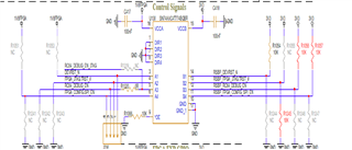
I'm using SN74AXC4T774BQBR at a design that translate 3.3V signals from Raspberry Pie (RSBP) side to 1.8V at FPGA side.
At 2 different boards this device stop functioning for a particular signal.
VCCB is 3.3V ; VCCA is 1.8V ; Dir1..4 = GND ; OE = GND via 10K resistor
One signal is connected to pin14 (B1) with a 3.3V 10K pull up - it is floating from RSBP side.
Instead of getting 1.8V at pin 3 (A1) I'm getting '0'
I've measured the resistance between that pin to GND and got 150 ohm. I've measured the resistance between this signal and 3.3V and got 900 ohm instead of the 10K (of pull up).
After removing the pull up I've measured 1K.
Clearly something damaged the buffer of B1 and although not driving by any signal and actually was floating, the potential was '0' thus A1 had '0' as well.
Either removing the device or either disabling it by OE=3.3V solve the problem and now pin A1 got it's '1' via 1.8V pull up.
I don't expect that pin B1 got higher than Absolute maximum rating (4.2V) as it was driving by RSBP (3.3V), moreover - other signals such as B3, B4 are connected the same but didn't malfunctioned