This thread has been locked.

If you have a related question, please click the "Ask a related question" button in the top right corner. The newly created question will be automatically linked to this question.

CD4093B: Logic forum

Part Number: CD4093B

Hi,

I have trouble to correctly set the CD4093 initial status. I use CD4093B to implement battery cutoff and latch function. See my schematic below.

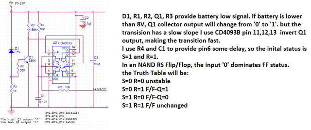
However, when I test the circuit, After startup (at Vin=10V), I don't get what I expect (initially S=1, R=0, Q=0;when C1 finishes charging S=1, R=1, F/F status unchanged, Q remains 0) . what I get is Q=1.

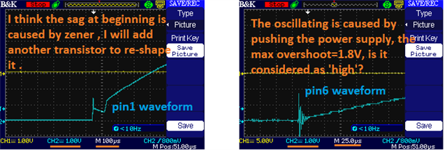
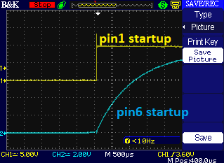
I check the startup waveform, nothing is wrong, see below waveform captured.

I am frustrated. Please help.

Thank you very much.

Chang Cao 

  • Hey Chang,

    I would need a bit more information to really be able to say for certain what the issue is. Such as a signal of the Q1 collector pin. 

    My best guess however, is that Vin is dropping below the diode breakdown voltage (7.5 V). This can just be due to tolerances of the diode or even the transistor. As the Vbe would be around 0.6V. 

    The only way for Q=1 is if S=0. S=0 only if Q1 is turned on which is how I came to this conclusion. 

  • Hi, Albert: 

    The Q1 collector voltage is 0.24V measured by meter. However I notice that the waveform has some abnormality if I zoom-in the time/voltage scales. I think it is caused by zener behavior and bouncing of pushing the power supply button.

    Thanks.

    Chang

  • The test is under Vin=10V, the maximum overshoot is 1.8V.

    According to datasheet VH is only 1.2V, then I can't test it. because when I push the power supply button, the circuit experiences '1'--'0'--'1'--'0' ....by BUTTON BOUNCING, the circuit is already fault latched when finish startup.

    Can I add de-bounce on CD4093B, such as cap?

    Thanks

    Chang

  • I plan to add another transistor inverter to re-shape zener output (don't use CD4093B one NAND as inverter.) And will change the pin6 charging resistor from 10K to 100K (increase the charge time constant for reducing the overshoot caused by power switch bouncing.

    If it is still no good, is there any NAND (or NOR) chip has regular VH=0.7VCC? I guess CD4093B has hysteresis feature, so Vin(min) is low

    Thanks.

    Chang

  • Hi Chang,

    Today is a US holiday so there will be a delay in responses. Our team will look into this and respond tomorrow. 

  • Hi, Albert:

    Fix the problem.

    1. Pin6 charging resistor changes from 10K to 100K, make the overshoot lower.

    2.Add another transistor for re-shaping zener output. However I can't use transistor as inverter then use 1 NAND gate inverts again. Must use transistor as same-polarity output and connect to CD4096 pin1 directly. Probably the transition time causes issue.

    Thanks.

    Chang