This thread has been locked.

If you have a related question, please click the "Ask a related question" button in the top right corner. The newly created question will be automatically linked to this question.

SN74LV4046A: SN74LV4046A as frequency multiplier

Part Number: SN74LV4046A

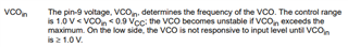
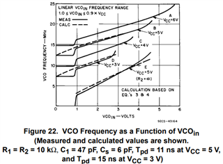
Hello, I am considering using the SN74LV4046A to multiply a base frequency in the order of the 10s kHz to obtain a variable frequency between 2.4 and 9MHz. The reference clock is generated by a microcontroller and the VCO output clock feeds an FPGA which divides it by 128 before sending it to the compare input of the SN74LV4046A. I read the AN "CMOS Phase-Locked-Loop Applications Using the CD54/74HC/HCT4046A and CD54/74HC/HCT7046A" and I was able to prototype a circuit using a breadboard which works but it is not very stable. In my circuit, C1 is 120pF, R1 3k and R2 is open. First I have noticed that when the VCO control voltage drops below 1V (about VCO output freq 2.5MHz), the VCO ouput frequency drops to some hundreds of Hz. Does this corresponds to the 1.1V voltage limit defined in the datasheet? For some input frequencies, I can see the output frequency oscillating as if the PLL is not locking. I tried different combinations of C1 and R1 but I was not able to improve my circuit. I also noticed that only compare output 1 and 2 work. Is my frequency range specification outside what this component is able to do? Many thanks

  • Hi Matteo,

    I have paged a device expert. He is out of the office today so we will try to get to later this week.

    First I have noticed that when the VCO control voltage drops below 1V (about VCO output freq 2.5MHz), the VCO ouput frequency drops to some hundreds of Hz. Does this corresponds to the 1.1V voltage limit defined in the datasheet?

    I'm not familiar with this part but I would assume that it is indeed related to the lower bound of 1.1 V for the VCO operating voltage linearity range. Outside of that, the behavior can be unpredictable.

    Best,

    Evan Su

  • Hi Matteo,

    VCOin should be greater than 1V.

    Based on below Cure E, we can try R1 = 10kΩ and C1 higher than 47pF, this will shift the cure downward to support 2.4MHz. 

  • Hi , thanks, I forgot to mention that I am powering the chip at 3.3V since my FPGA VCCIO is 3.3V.

    I have tried C1 = 47pF and R1 = R2 = 13k but i did not get the desired range. I started increasing the C1 and I found that with the following components I get closer to the range: R1 = 7k5, C1 = 80pF, R2 = OPEN. Now, for VCOin 1V I get 2.5MHz, for 3.3V I get 8.8MHz. 

    Even though I am close to the desired range I would like to be able to use the datasheet information to analytically find the component values to fine adjust it and make sure I am not using improperly the component. I also noticed from the oscilloscope that when I vary the reference clock from min to max frequency, the VCO output does not always follow smoothly but sometimes it has a stepping variation.   

    I have also noticed that the SIGin and COMPin (coming from the frequency devider counter) signals are not perfectly aligned in phase but there is quite a lot of jitter that is reflected on the VCOout. The higher the frequency, the higher the jitter. Does this mean that the PLL is not completely locked? At the moment as first order RC filter I am using R=5k7 and C=1uF. If I try to use COMP3, the situation gets worse (in my initial post I said that only COMP3 did not work but I probably did something wrong). 

    I should also point out that the prototype I am using is not ideal since I have flying wires from MCU and FPGA to the breadboard, however, I am not sure how much this could affect the circuit performance. 

  • Thanks , keep me posted. 

  • Hi Matteo,

    You have to use 5V so as to support the frequency range of 2.4MHz to 9MHz. From Figure 22, it is obvious that with 3V supply, you won't have enough VCOin tuning voltage to support 6.6MHz tuning range.

    SIGin is coming from external source, it should be stable source. When the PLL is lock, COMPin has the same frequency as SIGin, they should synchronize with some phase different. When the PLL is unlock, COMPin frequency is different from SIGin, they will not synchronize anymore.

    Using breadboard and flying wires may not be ideal for a prototype. At least, try solderable pcb breadboard and use shielded wire.

  • Hi , thanks for your reply. The need of translating from 3.3 to 5 and the other way around makes things more complicated than I expected. In fact, I would need to translate the reference clock to 5V and the VCO output to 3.3v . I would like to try and use it at 3.3V at the cost of decreasing the output  range. The plot you shared shows the output frequency as a function of the control voltage for a precise set of components. However, I did not find anything in the application note preveting from setting a lower frequency than the one showed in the plot. 

    I do understand that having a proper PCB would be better, I will try to improve the setup and see if something changes. I will open the loop and use only the VCO to make sure it works and then I will close the loop again.

  • Hi Matteo,

    Curve E is close to your frequency, that's why I took it as an example. This device can be configured to work at a much lower frequency. The application note has some examples that will walk you through the calculation. 

  • HI , as I mentioned, I tried to use only the VCO using a potentiometer to pin 9. What I have noticed is that even under these conditions the VCO output frequency has a lot of jitter. Therefore I think that the jitter I was experiencing with the closed loop is intrinsic to the VCO. Is this the normal behaviour of this chip?

    I m using 5V VCC, C1 is >40pF and R1=12kOhm.

  • Just an additional information, I have built a circuit using the 74ls624 VCO and wow, the output frequency is very stable with no noticeable jitter. I have closed the loop and designed a discrete D flip flop phase detector and the performance is great, I get the 2-9MHz locking range.

    It´s a pity the 4046 does not show the same stability since it would be the ideal solution for building a PLL given its integrated phase detector. Is this a well known issue?

  • Hi Matteo,

    I don't think the integrated phase detector is causing issues, I also don't see similar issue in past E2E posts. 

    Anyway, good to hear that you have got a solution. 

  • Hi Noel, I don´t think the 4046 phase detector is an issue. The 4046 VCO itself shows performance in terms of Jitter when in open loop. On my setup I have both the 4046 and LS624 next to each other and for the same center frequency the 4046 has a huge amount of jtter while the LS624 does not. To me it seems weird sicne the 4046 is widely used and wanted to know if there might be something I am doing wrong.

  • Hi Matteo,

    I am not sure, maybe the 4046 is sensitive to layout, maybe your problem will get fixed if you have a real board instead of bread board.