Hello,
As previously posted and deleted, I did ask if F in/out was special or had some other functions and the answer was no.
Now I'm tstill rying to fix an issue with F input/output on CD4505B where F out can't get at 0V when F in is at 0V .
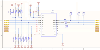
I do have the following connections:
1- 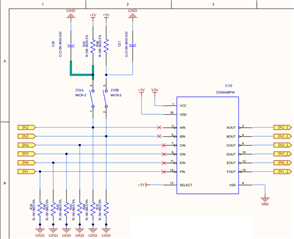
2- 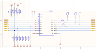
Description of the issue:
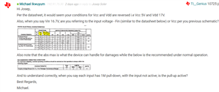
When connecting a NO push button on input 13 and 14 to GND, Fin and A in signals are 5V from the pull-up, when pushing the button both inputs go down to 0V and output also goes down to 0 V. However, when the push button is not connected directly, using a cable (more than 30cm), F in (In13 signal) goes down to 0V but F out goes down to 4.5V instead of 0 V. But if we do replicate the circuit on In14 (A in), the output (A out) goes down to 0 instead of the 4.5V we do get on F out.
When transient testing, F gate does not work properly (neither In1 nor In13) .
On both cases, it gets up to 200ºC after a few seconds .
On the previous question i did post, I was told to put a Capacitor on Vcc and Vdd since F gate was the farthest gate from source.
After modifying the circuit, results got worst, F out could not get under 4.8V when F in was 0V.
Also have tried to put a capacitor at the F in and A in (In13 & In14), but F gate seems more sensible and even with a 100n capacitor In13 (Fin) does not work and can't make F out 0V.
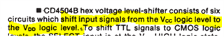
According to data sheet, on CMOS-CMOS low lvl is under 1.5V and TTL-CMOS lov level is under 0.8V.
Notes:
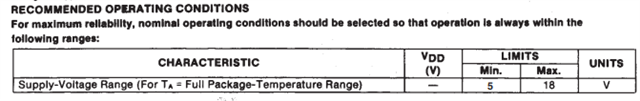
- Vin = 17V (16.8V).
- All outputs are connected to a micro controller.
- All inputs have a pull-down of 1M .
- 5V input signals had been used on tests. (Input signals range from 0-3.5V to 0.16V).
- Datasheet .
- Inverted signals is not an issue, since i can swap them inside the micro controller.
- All voltages are DC.