


Part Number: CD74HC367
Other Parts Discussed in Thread: SN74HC367
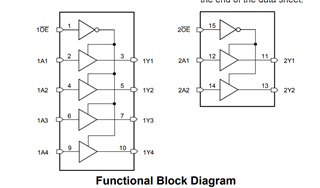
The above functional diagram is not matching with the pin configuration.
Functional block diagram: PIN 9 -input & PIN 10 -output
Pin configuration: PIN 9 -Output & PIN 10 -Input
Which one is correct? Either I need to refer functional diagram or pin configuration?????

