This thread has been locked.

If you have a related question, please click the "Ask a related question" button in the top right corner. The newly created question will be automatically linked to this question.

TXB0106: Device malfunction, maybe related to OE pin

Part Number: TXB0106
Other Parts Discussed in Thread: TXU0304, TXU0202, TXU0101, SN74LVC125A, SN74AXC4T245, SN74LVC2G34

Hello,

I'm trying to interface a modem (uBlox SARA 422S) to an ATmega1284P through a SPI/RS232 transceiver (PI7C9X760).
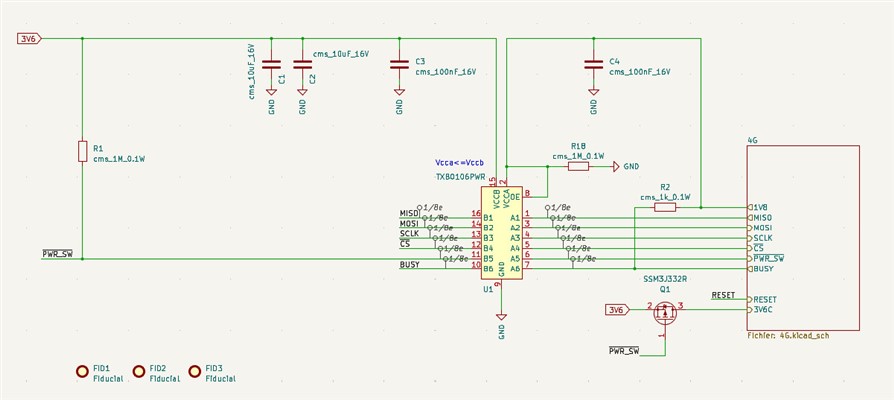
1.8V (line 1V8) is provided by modem when it is running (PWR_SW pull down and RESET done). Modem uses 1.8V logic. Thus PI7 is powered by 1V8 line.

TXB0106 is between processor and SPI/RS232 bridge as it provided isolation between SPI bus and PI7 bus.

In this configuration, TXB0106 doesn't run as expected. I have read again datasheet and I have seen that OE should be tied to VCCA after VCCA and VCCB are stable. Is a simple reset circuit (RC) enough to generate OE signal ? For example this kind of reset:
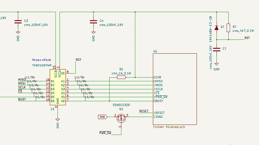
And can TXB0106 run in this configuration?

Best regards,

JB

  • If you do not care about the state of the outputs during power up, you can tie OE directly to VCCA.

    Anyway, the problem is that the TXB works only with small capacitive loads (< 70 pf) and with weak pull-up/-down resistors (≥ 50 kΩ). You have unidirectional signal, so you should better use unidirectional translators like the TXU0304 or TXU0202.

  • Thanks for your answer. I have tried to use TXB as outputs _and_ inputs can be set in high impedance. Datasheet of TXU shows that only output can be set in high impedance.

  • CMOS Inputs always have high impedance.

  • Datasheet of TXU0101, page 20:

    "This device has 5 MΩ typical integrated weak pull-downs for each input."

    5 MΩ are too low for my application (2.1 µA).

  • Hi Joel,

    To help clarify, are you referring to the input leakage current or the drive strength of the device?

    Note that an input impedance of at least 10 times the source impedance is a good idea to prevent significant loading. Could you help double confirm this isn't the case? I.e is your 3.3V signal with >500K ohms impedance? Hence, with the TXU's 5Mohms, you get 3.3V * ( (5M) / (5M+500K) ) = 3V as the input voltage and with a typical driver signal of 100K to 160K (I suspect this is your case), the input voltage at the TXU's input will be about 3.2V.

    If different, please help clarify what your application requires. For drive strength, see below, thanks.

    Best Regards,

    Michael.

  • If the TXU's input leakage (up to 2 µA) is too high for your application, use translators like the SN74AXC4T245. For translating to a lower voltage, you can also use any buffer with overvoltage-tolerant inputs, such as the SN74LVC2G34 or SN74LVC125A.

  • Input current only. Level translator is used to connect a modem (1.8V side) to an ATmega (3.6V). System runs with a Li cell. Modem is only powered when system has to transmit data (data are transmitted on event, maybe one packet per month).

    I cannot disconnect modem, it is only switched off by PWR_SW signal. I can force SPI CLK to 0, but not MOSI line that remains high even if CPU is sleeping. Indeed, I cannot unconfigure SPI as some devices don't support SPI unconfiguration. With 5 MR static resistor, idle current on MOSI and CS lines will be 3.6/5000000=720 nA (each line) + input leakage current (2 µA) as EO is tied to GND. 3.5 µA...

    Best regards,

    JB

  • The pull-down resistor current is already included in the input leakage current specification. (At high temperatures, the CMOS leakage current is higher than that through the resistor.)

    Below about 70 °C, the actual leakage current of the SN74 devices will be orders of magnitude lower than the specified maximum.