This thread has been locked.

If you have a related question, please click the "Ask a related question" button in the top right corner. The newly created question will be automatically linked to this question.

TXS0102: How to drive a high capacitance load without oscillations

Part Number: TXS0102
Other Parts Discussed in Thread: TMUX1208, P82B715, TCA9617B, P82B96

Hey,

We are experiencing oscillations in our I2C communication system since integrating the TXS0102 level shifter into our design. The oscillations are the result of the one-shot as described in the data sheet section 8.3.3 "it is recommended that this lumped-load capacitance be considered to avoid O.S. retriggering, bus contention, output signal oscillations, or other adverse system-level affects."

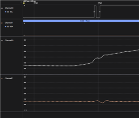
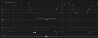
Here is a oscilloscope capture of the oscillation on SCL, and the cross-talk onto SDA.

Output oscillation waveform capture

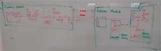
We have several sources of bulk capacitance: ESD diodes, a TMUX1208, 1.25 meters of fixed cabling, a customer selectable additional 1.25m-2.5m of cabling. We estimate 400pF to 800pF of equivalent capacitance. (I can measure it tomorrow.)

When the capacitance is on the high end, we experience this oscillation. We identify this oscillation as a high frequency of I2C communication errors reported by our I2C master controller. 

TI Application report "SCEA044–June 2010" titled "A Guide to Voltage Translation With TXS-Type Translators" states: "With capacitive loading >70pF, the TXS-type devices will still successfully operate at lower data rates"

What are the design considerations required to successfully operate this device with capacitive loading >70pF? 

Best Wishes,

Erich

  • Hi Erich,

    TI Application report "SCEA044–June 2010" titled "A Guide to Voltage Translation With TXS-Type Translators" states: "With capacitive loading >70pF, the TXS-type devices will still successfully operate at lower data rates"

    Similar to the supporting documentation, help lower your data rate as low as possible until the I2C communication passes, thanks.

    Best Regards,

    Michael.

  • The data rate is not the source of the failures, its the oscillation. The oscillation is causing I2C devices to mis-count clock pulses, or is coupling into the data line and causing devices to mis-read the data signal. 

    To successfully drive this capacitance, I need to eliminate this oscillation. 

  • Capacitive loading just slows down the edges. The oscillations are a different problem; they are triggered by ringing on the lines, which is caused by capcitance and inductance. If you cannot change the characteristics of the system, then you cannot use the TXS.

    For such high bus capacitances, you should use I²C buffers like the TCA9617B. (The TXS is not a buffer.) When exceeding 400 pF, consider cable extenders like the P82B96 or P82B715.

  • Hi Erich,

    Out of curiosity, could you help share schematics / block diagrams? i.e do you have resistors externally while driving 400pF to 800pF with the device?

    Note that Clemens also clarified as I actually do not see any oscillations in the provided waveform. Perhaps you are referring to the reflections.

    You may also see section 6 of Do’s and Don’ts for TXB and TXS Voltage Level-Shifters with Edge Rate Accelerato for some recommendations, thanks.

    Best Regards,

    Michael.

  • Hey Michael, 

    Thank you for the response. Here is a basic block diagram of our I2C bus. I just drew the SCL line, but the SDA line is the same:

    DNI = do not install

    My scope is more of a logic analyzer. The analog sample rate is too low to see the oscillations well, but the digital section shows them better:

    We have demonstrated a solution using a cable extender, but the solution is cost prohibitive. 

    We have already deployed products with the TXS. We will certainly look at alternate sources going forward, but are looking for a strategy to salvage produced products. So far the alternate sources we have looked at are not pin compatible. 

    We have had some luck with filtering the ripple at the TXS by placing additional capacitance and impedance at its input.

  • Hi Eric,

    I suspect you are not translating at fast data rates for the estimated loading as I am surprised to see translation at 800pF.

    Within the control module, TXS would translate just fine from I2C to TMUX. I.e probing the outputs before the TMUX.

    For your reflections, please also see below FAQ as you may use series dampening resistors. Help also ensure your input transition rate is within the datasheet's recommendation for faster transition rates, thanks.

    1. [FAQ] What happens when I connect a logic device's output to a 50 ohm transmission line?

    Best Regards,

    Michael.

  • This is silly to say, but we realized after doing a design review that the I2C master has +5V compatible TTL inputs, and we do not need the translator. Our current plan is to remove the part and jumper across the pins with resistors. 

    We are running the serial clock at around 200KHz. The I2C master will adjust the clock rate based on the rise time. 

    I think I am correct to model the TMUX as a resistor, a 3 to 7 ohm one based on the data sheet. I would not expect to measure radically different signals on the input and output side of the TMUX, because of this low impedance.

    Thank you for the transmission line topic, that was informative.