This thread has been locked.

If you have a related question, please click the "Ask a related question" button in the top right corner. The newly created question will be automatically linked to this question.

TXS0108E: TXS0108E

Part Number: TXS0108E

Hi 

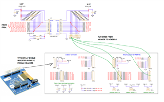
We are using TXS0108E this level translator on our board for TFT display parallel bus interface (DBI-B) at 1MHz frequency.

our MCU is operating at 1.8V and we are level-translating these signals to 3.3V to connect to the TFT display which is configured for 3.3V IO voltage.

In this case, the TFT display is not fully working properly. Please see attached image.

But when we configure the TFT display IO voltage to 1.8V (i.e. now MCU is also 1.8V and TFT also 1.8V with level translator) display works fine. 

Please suggest why this level translator does not work in 1.8V to 3.3V configuration.


Thanks

Santosh

  • Please show the schematic, including all devices that are connected to the TXS.

    Note that the TXS does not work at high speeds with long traces or cables that would increase the load to more than 70 pF. Please show an oscilloscope trace of the 3.3 V signal, but I guess that the rising edges are too slow.

  • The fly wires might be too long.

    Please show an oscilloscope trace of the 3.3 V signal.

  • hi 

    please see the scope capture of "write signal" for 1.8V and 3.3V operation

  • There is ringing on the line that looks like the beginning of a rising or falling edge. This triggers the TXS's edge accelerators. So this ringing results in strong oscillations.

    You cannot use the TXS with such long cables.

  • but the setup works with 1.8V. what is the difference from TXS when it is 3.3V or 1.8V? I mean why is this noise on the rising and falling edge only for 3.3V on VCCB side

  • Hey Santosh,

    In addition to Clemens' response, operating at higher voltage nodes also scale into bigger overshoots/ undershoots. It is noticeable during 1.8V operation, but does not seem problematic until 3.3V operation occurs. Are the signals per channel bi-directional or is it fixed direction? If they are fixed direction signals per channel, an alt. level translator can be used, such as the AXC8T245 or the LXC8T245 that has configurable direction controlled pins.

    Regards,

    Jack 

  • Hi Jack thanks for the suggestions. Signals are not bi-directional but our board is designed for multiple configurations so the same signals can be configured as bi-directional in some other configurations but they are unidirectional when TFT display is connected. alternate  level translators AXC8T245 or the LXC8T245 are not drop-in compatible with TXS0108E could you please suggest any other alt parts that are pin compatible with TX0180 as we have built the PCBs already

  • There are no pin-compatible unidirectional alternatives to the TXS0108E. (The TXU0x04 would be P2P for the TXB0104E.)

  • Load on the B-side of TXS should not be more than 70pF? 

    this include PCBtrace+fly wire capacitance+Header pin capacitance+TFT display pin input capacitance?

    Under what conditions do TXS edge accelerators trigger? and what if they trigger? why it is not good if edge accelerators trigger?

    please suggest

  • Hey Santosh,

    Yes you are correct- having this high of a capacitive load (PCB traces, connectors, and device capacitances) will be problematic as it will cause oscillations, similar to that you have seen in the waveforms. The internal edge accelerators of this device help speed up the rise time of an input logic HIGH so that a faster LOW to HIGH time can be achieved (helps support higher data rates). However, when used with long cabling, you can cause reflections on the data line that can potentially retrigger this edge accelerator, even if no input signal was generated to the device. 

    Here is an app note that goes more in depth of the TXS device:

    Do’s and Don’ts for TXB and TXS Voltage Level-Shifters with Edge Rate Accelerators

    Regards,

    Jack 

  • Hi Jack and Clemen

    This screenshot is from TX0108E Eval board schematics. Here they are using pull-ups and capacitors on the level translator IOs. Why is this? Don't these 100nF capacitors load the TXS108 IOs beyond their 70pF output load capacitance? Please suggest.

    Because when we also added pull-ups of 1.8K and a capacitor of 100pF on the WRITE signal we saw that ringing on the falling edge is gone and the display is working sometimes.

  • Hey Santosh,

    The 100nF values are not populated on the TXS evaluation board. They only resemble a place to populate capacitors for system tests.

    Are you able to provide the waveforms of the 1.8kohm pullups and 100pF loading condition since you mention that the case is only working some of the times? It is also suggested to test with other connectors/ cabling as big ground loops can create additional inductance that can also cause ringing on the rise/ falling edges as well.


    Regards,

    Jack 

  • Hi Jack

    Below are the waveforms with a 1.8K pullup and 33pF cap on D0 signal FYR. With this rework, it is working.

    we have mounted a 1.8K pullup and 33pF cap and each signal. Please suggest how these additional capacitors and pullups make it work at 3.3V.

  • Hey Santosh,

    The 33pF capacitors on each line are within spec of the <70pF loading condition. Having the stronger pullups (1.8kohms) in parallel with the internal 10kohms allow for a stronger drive strength, but with the raised VOL levels as shown in the waveform.

    Regards,

    Jack 

  • Hi Jack

    33pF is an additional capacitor along with PCB trace capacitance, connectors, and device capacitances, right? Initially, it is mentioned that the display is not working maybe because of the capacitance loading by long traces/wires and connectors is >70pF. but how did you consider only 33pF as load capacitance now? are you not considering the PCB trace capacitance, connectors, and device capacitances?

    Thanks

    Santosh

  • Hey Santosh,

    It is just a general rule of thumb and good practice to keep the capacitive load to a minimum and under <70pF as it couples on noise onto the data bus (can be amplified by unstable power supplies and GND) and limits the maximum achievable data rate. Keeping the total capacitive load under 70pF also allows the round-trip delay of any reflection to be less than the one-shot duration as well. Are the current waveforms acceptable for the system? If it works on your system then it is OK to leave as is.

    Here is an FAQ on long traces and the impact of the transmission line. 

    Thanks,

    Jack