This thread has been locked.

If you have a related question, please click the "Ask a related question" button in the top right corner. The newly created question will be automatically linked to this question.

SN74LVC3G17: SPI Configuration for Long-Distance Transmission at 0.5MHz to 2Mhz Data Rates using CAT5 Cable & Buffers at both end

Part Number: SN74LVC3G17
Other Parts Discussed in Thread: SN74AUP3G17, SN65LVDT41, SN74HC14, SN74HCS125, TXU0304

Hello Everyone,

I am working on a project that involves a 1 to 2 meter transmission distance of SPI communication. The application requires transmitting 3200 samples of 16-bit size from 3 axes every second, which amounts to a data rate of approximately 154 kbps.

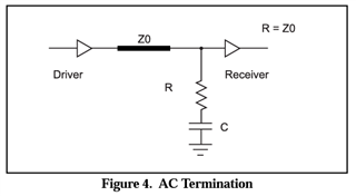
My SPI configuration includes a single master and single slave setup with 4 wires (MISO, MOSI, SCLK, and CS). I plan to use CAT5 cables for this purpose. Given the cable's inherent characteristics and the distances involved, I anticipate potential challenges with signal integrity due to signal reflections, EMI, and other factors.

To mitigate these challenges and achieve robust SPI communication, I am considering the use of SN74LVC3G17 buffers with Schmitt trigger inputs at both ends of the SPI connection. This buffer is designed to handle a supply voltage from 1.65V to 3.6V and provides over-voltage tolerant inputs, balanced outputs, and is very high-speed compatible (tpd 5-10ns).

I am also contemplating the clock frequency for this configuration. I understand that a lower clock frequency would provide better signal integrity due to lower susceptibility to signal degradation. However, it could also limit the data rate. I am currently considering 0.5 MHz and 2 MHz as potential clock frequencies.

I'd appreciate if anyone can share their experiences, suggestions, or concerns related to the following questions:

1. Is the SN74LVC3G17 a suitable choice for the buffer in this application?
2. What are the key considerations I need to take into account regarding signal reflections, especially when using such buffers in my configuration?
3. Would a clock frequency of 0.5MHz too low of a choice considering the data rate and potential signal integrity issues? Or would 2MHz be more optimal given the configuration?
4. Does anyone have experience or suggestions regarding SPI communication over similar distances, and if so, any specific recommendations or potential pitfalls to avoid?

Thank you in advance for your insights and help!

Best Regards

  • The clock frequency should be as high as necessary, and as low as possible. I do not know how much overhead your protocol has. Please note that a lower clock frequency, by itself, does not increase the robustness (a false clock pulse induced by noise will get through anyway), but allows you to filter out more higher frequencies.

    The SN74LVC3G17 is a good choice, but its high drive strength results in very fast edges. You want at least source termination, but to filter out high-frequency noise, you could use R-C filters. So the buffer's drive strength does not matter, and you could just as well use the SN74AUP3G17.

    CAT5 cables are designed for differential signal pairs. To avoid crosstalk, you should never pair two different signals. You can use the same signal for both lines in a pair, or pair a signal with VCC or GND.

    Consider using a differential protocol like LVDS. There are integrated multi-channel transceivers for SPI like the SN65LVDT41/14, or you can use multiple smaller transceivers.

  • Hello Clemens,

    Thank you for your feedback. Yes, we have designed one system with AM26Cxx series differential driver & receiver pairs for MEMS sensor to MCU connection.

    For this application, we cannot use differential drivers as the cost is prohibitive, but buffers seem to be within the budget. We are using CAT5 cables for their shielding ability. I have noted your suggestions for paring within the cables with Vcc & Gnd. Can you suggest some references for us to cross-check our source termination resistor calculations?

    I find it safe to assume this is one of the most common use cases that designers & engineers may be facing to interface SPI from sensors, ADCs over 1-2m distance. Is there some benchmarking that TI can publish? We do not always have access to high-precision Osciliscope for testing the performance, maybe you/your team can publish a simple single Master-Slave 4-wire configuration with 0.5, 1, 1,5 & 2m distance use cases with different cable types & other key features that influence the design decisions.

  • The total output impedance of the buffer (the buffer's own output impedance plus the source termination resistor) should match the characteristic impedance of the cable. CAT5 is specified for a differential impedance of 100 Ω, but the single-ended impedance is usually not specified, and typically is somewhere between 60 Ω and 80 Ω.

    It might make sense to have buffers at both ends. Consider the SN74HC14 or SN74HCS125.

  • Hello Clemens,

    Which is a better option for a configuration where we are using buffers at both the end of the SPI - one at the Master & other at the Slave?

    SN74HCS125 or SN74LVC3G17?

    I noticed the IOL & IOH for these are 7.8mA & 32mA.

    Is this a wrong assumption that a higher IOH/IOL device would be better choice?

  • You have four signals, so you should use four-channel buffers.

    Higher drive strength does not matter when you use source termination or R-C filters.

  • Hello Clemens,

    Can you share detailed design procedures/application notes/reference designs that can help us properly terminate potential reflections?

    I found these FAQs by  very informative.

  • If you want to match the line impedance, then compute the buffer's worst-case output impedance with VOL/ IOL at whatever supply voltage you're using, and estimate the typical output impedance as roughly half that.

    However, the purpose of matching the line impedance is to avoid reflections while still allowing as high a signal frequency as possible. If you have a low-frequency signal and want to filter out as much higher-frequency noise as possible, then you would not match the line impedance, but add R-C filters with a higher impedance. For example, for a 2 MHz clock, an R-C filter with a bandwidth of > 10 MHz can be constructed with R = 1 kΩ, C = 10 pF (the effective R and C are somewhat higher because of the buffer's output impedance and the receiver's input capacitance). The exact behaviour depends on the characteristics of the cable; you need to check the waveforms with an oscilloscope.

  • Hello ,

    Thank you for your as always crisp, to the point & insightful feedback & suggestions.

    We had another question for you, when trying to maintain the Signal integrity of the SPI signals over 1/2m cables, how well can buffers like TXU0304 be helpful when compared with SN74HCS125 at both ends?

    Your insights will further help us refine our approach before we test them with prototypes.

    Regards.

  • There is no practical difference. The TXU has higher drive strength, but this does not matter when you reduce it with a resistor.

  • Hello Clemens,

    We are then for our test prototype finalizing TXU0304 on both ends of the SPI bus.

    The configuration is as follows:

    SPI MCU Master (3.3V) > TXU0304 (3.3V to 5V) ~~~ SPI BUS ~~~ TXU0304 (5V to 3.3V) > SPI Sensor Slave.

    Objectives:

    1. Improve Noise margins by level translation from 3.3V to 5V on the SPI Bus (Shielded Cables)
    2. Enable longer distance transmission (0.5m to 2m)

    We are planning to use R-C filters as per your suggestions with R = 1 kΩ, C = 10 pF to eliminate higher frequency noise from the bus.

    Follow-up question:

    1. Our maximum clock speed shall be 2MHz by design, will a lower cutoff RC filter (4MHz < Fcutoff < 10MHz) add any significant benefit in performance?
    2. We are using AC termination as attached:

    This is what you meant in your suggestion to eliminate the higher frequency noise from the SPI bus, right?

  • The RC filter bandwidth applies to analog signals, and the cutoff frequency specifies the frequency at which a sine wave gets attenuated by 3 dB, i.e., by half. To transmit a digital signal (a square wave), you need more bandwidth; this is why I've used 10 MHz for a 2 MHz clock.

    AC termination tries to match the impedance; this would not filter out high frequencies. An R-C filter consists of a resistor in series (like a source termination resistor) and a capacitor to ground.

  • Okay,

    Isn't the R = 1 kΩ in series too much for the SPI bus? I am unable to interpret your suggestion here, can you help us with a reference design that we can follow through?

  • Why do you think it's too much? Together with the capacitor, it slows down the edges.

    It might be too much if the SPI bus is so long that it adds too much capacitance.

  • Hello ,

    As per your suggestion, we will add the RC to our above system as illustrated in the attached figure below.

    Specifications:

    1. SPI Full Duplex with 1 master & 1 slave over 0.5m to 2m distance
    2. Max clock frequency 0.5MHz to 2Mhz
    3. Cables: Shileded Twisted Pair with Data paired with power lines (MOSI + GND & MISO + Power)
    4. TXU0304 or SN74HCS125 at both ends of the SPI Bus cables to improve noise immunity with:
      1. Schmitt trigger inputs
      2. Level translation from 3.3V to 5V
    5. R-C Filter with Rf = 1 kΩ, Cf = 10 pF to eliminate higher frequency (>10MHz) noise from the bus

    Questions:

    1. Do we place the RC filter as close to the driver pins of the Buffer OR the MCU?
    2. Do we need RC FIlter only on Source end or both? (Application Note from TI) has it on both as attached below when using RS-4xx pairs

  • 1. Yes.

    2. Two filters would combine to reduce the maximum frequency.

    Please note that traces and cables have a capacitance of very roughly 1 pF/cm, so 2 m will result in about 200 pF, so you can reduce or omit the discrete capacitor, and have a smaller resistor of somewhere between about 50 Ω and 100 Ω. You should compute this with the actual values you're using, and check with an oscilloscope.