This thread has been locked.

If you have a related question, please click the "Ask a related question" button in the top right corner. The newly created question will be automatically linked to this question.

LSF0204-Q1: switch saturation levels

Part Number: LSF0204-Q1
Other Parts Discussed in Thread: LSF0204

Team,

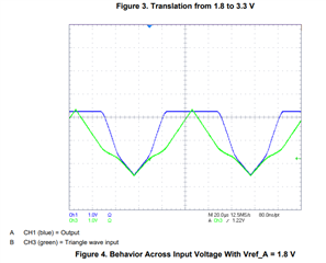
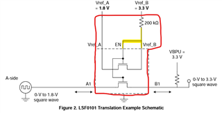
I'm surprised to not find more data on the saturation level of the input-output switch of this family of level shifters in the datasheet. from https://www.ti.com/lit/an/slva675b/slva675b.pdf figure4 . I'm guessing that in the HW configuration described figure 2 of the same document, I'm guessing that the opening of the switch starts around 0.8V to end around 1.3V: am I correct ?

Is there a way to find this information anywhere else?

  • For voltages below Vref_A, the LSF works like an analog switch. (For voltages above Vref_A, the switch is open, and the output voltage is determined by the pull-up resistor.)

    However, the LSF is not intended to be used for analog signals. Digital low signals are near 0 V; digital high signals are at Vref_A or higher. The threshold voltage of the MOSFET is less than 0.8 V (see table 8-2 in the datasheet), but this information is not relevant.

  • Clemens, thanks, threshold and saturation is still an interesting information to share I find. Can you please confirm on the triangular input figure above the gnd is at the bottom of the triangular waveform?

    thanks

  • According to the labels below, both curves use the same scale (1 V). It appears the top of the curves is 3.3 V, and the point where the curves diverge is near 1.8 V.

  • Clemens, ok thanks. Would the curve look the same if Bside is the input and Aside the output ?

  • Hey Olivier,

    Yes this behavior is similar to if B-side is used as input and A-side as output (this device is auto bidirectional and the drain/source of the FET can be used interchangeably.  You can also see the switch during normal operation in the logic minute video series.

    Regards,

    Jack 

  • thanks for the video, it's crazy how the simplest devices are usually the toughest to grasp. So typical FET threhold in both direction A>B as B.A is 0.8V. can we get any feel for the spread of this parameter against aging/process variation / temperature.

    this is critical for TIer1s to justify their deisgn to car oem.

    thanks 

  • Hey Olivier,

    The spread will be bounded within the datasheet specs as their values were taken across PVT under the testing conditions listed in section 8 of the datasheet.

    Regards,

    Jack 

  • Jack, thanks can you please point them to me in the datasheet ? thanks

  • Hey Olivier,

    The specs are can be seen in the switching characteristics such as tplh and tphl. The 0.8V threshold voltage itself is not specified in the datasheet- this is part of the design of the internal FET since it is in a diode- like configuration and is not required to know this Vth value in order to operate the device. The value of the RON is more crucial as they determine the timing specs and allow for lower VOL levels seen at the output.

    Regards,

    Jack 

  • thanks for the video, it's crazy how the simplest devices are usually the toughest to grasp. So typical FET threhold in both direction A>B as B.A is 0.8V. can we get any feel for the spread of this parameter against aging/process variation / temperature.

    this is critical for TIer1s to justify their deisgn to car oem.

    I agree - this device and ones like it generate more technical questions than most other device.

    The 0.8V threshold voltage itself is not specified in the datasheet- this is part of the design of the internal FET since it is in a diode- like configuration and is not required to know this Vth value in order to operate the device. The value of the RON is more crucial as they determine the timing specs and allow for lower VOL levels seen at the output.

    I agree with Jack here but thought I could provide a little more insight as to why you can (mostly) ignore the gate threshold in this circuit.

    The LSF010x series of translators only include transistors in the IC (dotted box), while the LSF0204 incorporates a bit more inside (red box). Ignoring the enable circuitry (since it doesn't affect the bias), the 200kohm resistor and external diode-connection of the bias channel are moved internal for the LSF0204, so it makes the translator easier to use by eliminating that external bias circuit.

    Because the channel transistors are on the same die, we can expect that their characteristics will remain very closely matched across PVT, and the gate threshold can essentially be designed out of the equation for the translation circuit. That is - assuming you have enough difference between Vref_A and Vref_B to provide sufficient bias -- which is at least 0.8 V:

    Speaking more mathematically:

    The gate voltage (ref to gnd) of the bias transistor will be:

    (Eq 1) V_G = VCCA + (V_tn + V_od)

    V_tn being the gate threshold voltage, and V_od being the over-drive voltage for the given bias condition.

    We assume V_od is very small since we bias at only a few micro-amps, so let's replace that with zero and we get:

    (Eq 1a) V_G = VCCA + V_tn

    Looking at any other channel transistor, the gate voltage is the same (they are wired together internally), so when determining the state of one of the channel transistors we can use the following:

    (Eq 2) V_GS = V_G - V_S

    V_G being the same as the first gate, and V_S being the lower of the two voltages between V(A1) and V(B1) in the drawing above.

    Substituting Eq 1a into Eq 2:

    (Eq 3) V_GS = VCCA + V_tn - V_S

    Device is in cutoff if Eq 4 is met:

    (Eq 4) V_GS < V_tn

    Sub Eq 3 into Eq 4:

    VCCA + V_tn - V_S < V_tn

    Subtract V_tn from both sides...

    VCCA - V_S < 0

    And rearrange a bit

    V_S > VCCA

    Which nicely explains how the device really works -- if the input is above VCCA, the nFET is turned off, and when the input is less than VCCA, the nFET is turned on.

    V_tn plays no part in the actual translation -- with the exception of having enough voltage difference between VCCA and VCCB to support it (at least 0.8 V).