This thread has been locked.

If you have a related question, please click the "Ask a related question" button in the top right corner. The newly created question will be automatically linked to this question.

CD4013B: CD4013B

Part Number: CD4013B

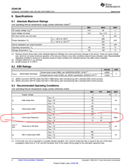
Dear Technical Support, attached is CD4013B datasheet and P.4 of the related datasheet, the circled area of P.4 shows that the " Clock Input Frequency " related data, and it listed the MIN. & TYP. data values, 

but not listed the MAX data value, 

I am wondering if there is a mistake on this data values, I think the MAX data should not be left open, the left-open data should be the MIN data instead, 

It is because for this kind of Logic Devices, there should be a MAX. Clock Input Frequency limit value, but should have no MIN. Clock Input Frequency limit, and this is because if the Clock Input Frequency is too high, then there is a possibility the data cannot recognized and shown correctly at the output of the device, 

Not sure if I am right on this? Please let me know if I am wrong and why I am wrong if convenient. 

Look forward to hearing from you when convenient. 

Thanks 

yenwu lo

 cd4013b-mil.pdf

  • Hi Yenwu,

    This should actually say "Maximum Clock input frequency". So this means the "Smallest" maximum clock frequency at Vdd = 10 is 8 MHz, but the typical maximum clock frequency at Vdd = 10 is 16 MHz.

  • Thanks for the explanation, Albert Xu1, I attached another file "Capture_P.4 of CD4013B datasheet_1.PNG".

    My question is:

    Since the current datasheet did not specify MAX value column area for Vdd=5V, 10V, 15V,

    so does this mean that the Max. input clock frequency for each Vdd case does not have max. limit?

    Does this mean that for each Vdd case, the input clock frequency can be any value without any upper (max.)  limit? 

    so if the input clock frequency is close to a value which is very close to infinitive value, this device still will be able to work successfully?

    I do not think this device will work when the input clock frequency reaches a value close to infinitive value, this device will work seccessfully.

    So I suggest the circled Max-column area should not be blank as it is now,  

    While the circled min. value area can be left blank, no need to specify, because when the input clock frequency is low, the device should still work without issues.

    Please help to confirm if I am correct or not? 

    If I am wrong, please let me know why I am wrong if convenient.

    Thanks

    yenwu lo. 

  • a typo corrected in this sentence above and copied below for your easy reference.

    I do not think this device will work successfully when the input clock frequency reaches a value close to infinitive value, this device will not work successfully in this situation.

  • Take three random CD4013B chips, call them A/B/C, and test them at 10 V.

    Chip A supports all frequencies between 0 MHz and 17 MHz.
    Chip B supports all frequencies between 0 MHz and 8 MHz.
    Chip C supports all frequencies between 0 MHz and 15 MHz.

    There are three maximum values. The value that is guaranteed to be supported by all chips is 8 MHz, the smallest of these, i.e., it is the minimum of the maximum values. "Minimum" means "at least", i.e., all chips are guaranteed to support at least 8 MHz.

    (As Albert said, the label should not be "clock input frequency" but "maximum clock input frequency".)

  • Thanks. Clemens, Your explanation is very clear for me, please close this case. Thanks again. yenwu lo