This thread has been locked.

If you have a related question, please click the "Ask a related question" button in the top right corner. The newly created question will be automatically linked to this question.

TXS0206: Vih and Vil specs

Part Number: TXS0206
Other Parts Discussed in Thread: TXS0108E

I'm considering using the TXS0206 in an application to interface an Intel Stratix 10 FPGA with 1.8V I/O to a 3.3V SD Card Interface.  I'm struggling to understand the TXS0206 Vih and Vil specs, especially on the low side.  The FPGA Vol is max 0.45V, but the TXS0206 requires Vil of only 0.15V.  Considering that 0.45V is a common 1.8V Vol for many devices, how is it possible to drive the TXS0206 low with any 1.8V output?

Similarly for the high side, the FPGA Voh is min 1.35V, but the TXS0206 requires Vih of Vcc-0.2V, or 1.6V for a 1.8V Vcc.  Considering that 1.35V is a common 1.8V Voh, how is it possible to drive the TXS0206 high with any 1.8V output?

I watched the videos explaining the operation of the LSF translators, which explain why the Vil is so low (to maintain Voh on the B-side of 0.4V, so there's about a 0.25V drop from A-side to B-side), but I can't figure out the corresponding reasoning for driving high.

Thank you.

  • Hey John,

    The reason lies behind the passive translation- switch based architecture of this device. For input signals below VCCA, the device acts as an analog switch, with direct connection from the inputs to outputs. For input signals above VCCA, the internal FET goes into high impedance, ultimately isolating the inputs and outputs. 

    The specified VIL/VIH are specified in datasheet to show the direct dependency of the input has on the output of the device. Note the VIL max value is required to be followed only if the expected VOL value is 0.4V. In other words, as long as the VOL of the FPGA + the voltage drop across the FET matches the VIL requirement on the SD Card interface, then this device can be used.

    Here is an FAQ and an app note discussing Factors Affecting VOL for TXS and LSF Auto-bidirectional Translation Devices that covers your question further. 

    Regards,

    Jack 

  • Jack,

    I read through the app note you referenced, as well as the A Guide to Voltage Translation With TXS-Type Translators app note.  I understand how the Vil/Vol works, and why Vil is so low.  And I can also understand how to figure out if this will work with my application, since it's all just a "pass through" design with a voltage drop.

    However, none of this helps me understand how it works when driving high, since the pass transistor is open, and the A and B sides are independent.  The TXS0206 datasheet lists Vih as Vcci - 0.2V.  In my application, Vcca is 1.8V, so this would make Vih on the A-side to be 1.6V.  But I'm driving this with a 1.8V CMOS output which has a Voh min of 1.35V.  How can I guarantee that my FPGA can drive the A-side data inputs?  Unlike driving low, the Vih requirement isn't set to ensure Voh is at the proper level.

    Since the pass transistor is off (presumably at Vcci/2), and since the inputs have pullup resistors, I would expect the inputs to eventually be brought up to the Vcci rails through the pullups.  So is the Vih requirement of Vcci-0.2V to ensure that the translator/oneshot is triggered?

    It seems that this situation is even worse on the SD Card side, for an SD Card at 3.3V.  According to the SD Card spec, Voh of the SD Card is min 2.475V, but the TXS0206 requires 3.1V.  That's over 1/2 V difference!  And this part is supposedly designed specifically for SD Cards.  So how does this actually work?

  • The oneshot triggers at lower voltages (about 30 % of VCCI).

    For all voltages up to the lower supply, the TXS works like an analog switch. As far as I can see, the VIH requirement does not make sense.

  • Clemens, that would be great if it's true.  Is that documented anywhere?  I see that for all of the TXS02 parts with the same architecture, Vih is always specified as Vcci-0.2V.

  • Hey John,

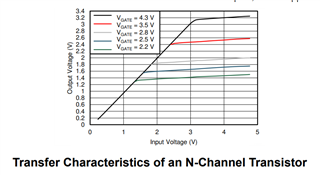
    Taking a look at the TXS010x datasheet (similar device in same family of translators), we see the following figure that indicates the behavior of the device as we scale the input voltage. Since this device is not a buffer, the output tracks the input until the FET turns off (when the input signal reaches ~VCCA). The VIH value in the datasheet simply guarantees an output high when the input signal reaches VCCI-0.2V. 

    Simply put, there isn't a designated "logic high" level or a "logic low" level that the device has, only that the FET turns off for input signals above VCCA. 

    Regards,

    Jack 

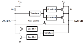
  • Jack, the TXS010x doesn't have the same architecture.  The TXS0206 has a translator and one-shot.  I agree, though, that on a rising edge, the output will follow the input until the pass transistor turns off (presumably around VCCA/2, or whatever the internal bias voltage is).  The question remains, though, at what voltage does the translator/one-shot trigger?

  • John,

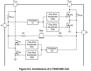
    The TXS0206 uses similar architecture to that of the TXS0108E, with a rising/falling edge one shot:

    Unfortunately, I cannot give exact values since we do not spec the threshold for when the one-shot circuitry is activated. However, it is likely to be around 30%~40% of VCC. 

    Thanks,

    Jack 

  • Thank you for all of the explanations so far... they're starting to help me understand how this would apply to my application.

    However, the TXS0108E still specifies Vih as Vcci-0.2V (for low voltages on the A side) or Vcci-0.4V (for Vcci above 1.95V on the A side, or all voltages on the B side).  My application has 1.8V on the A-side.  So is there any indication of where the Vcci-0.2V comes from, since when the input and output are high, there isn't really a connection from input to output?  I believe the output is just driven high by the internal pullup, and it should stay high as long as the input is above the threshold to turn the pass-transistor back on, which I would have expected to be around VCC/2 (based on some information I found that talks about the FET bias voltage in other similarly architected parts).  Based on that, the Vcci-0.2V (or -0.4V) doesn't seem to make much sense.

  • Hey John,

    I believe the output is just driven high by the internal pullup, and it should stay high as long as the input is above the threshold to turn the pass-transistor back on

    Yes, your understanding is correct. Recall that the VIH level is not a strict requirement for an input high signal, since there is no internal logic associated with the device as it is a passive switch. It behaves in a similar manner driving from ALeft right arrowB and BLeft right arrowA. 

    If you continue to have doubts, I would suggest to use the TXS0206A EVM to further test with your application & ensure that it meets your system requirements.

    Regards,

    Jack 

  • So I guess no one has an explanation as to where the Vih spec of Vcci-0.2V comes from or what it relates to?

  • If you continue to have doubts, I would suggest to use the TXS0206A EVM to further test with your application & ensure that it meets your system requirements.

    OK, lets suppose I get an eval kit and try it out. Here's what will happen...

    1) I'll setupVCCB with a 3.3V supply and VCCA with a 1.8V supply
    2) I'll drive the B-side input with a 2.5V input, which is VCCB-0.8V, and considered a valid Voh for a 3.3V SD Card output (2.475V), but violates the datasheet Vih requirement of VCCB-0.2V.

    If we see the A-side output switch to a logic high (as we expect), then all I will have proven is that this sample set of 1 far exceeds the Vih requirement. What are the chances that I'll get an eval kit with a part that just barely meets the Vih requirement and fails the test?

    Or how many eval kits do I need to test to get enough confidence that I can guarantee I can drive the inputs lower than Vcci-0.2V?

    Or is it that the Vih spec is just wrong?

  • Hey John,

    So I guess no one has an explanation as to where the Vih spec of Vcci-0.2V comes from or what it relates to?

    No, I do not have an immediate answer to this question at this time. 

    2) I'll drive the B-side input with a 2.5V input, which is VCCB-0.8V, and considered a valid Voh for a 3.3V SD Card output (2.475V), but violates the datasheet Vih requirement of VCCB-0.2V.

    What is the drive current (IOH) of the SD Card output with the 2.5V condition? Note that even though 2.5V is a valid VOH in the datasheet of your SD card, the IOH parameter also needs to be taken into consideration to realize your actual application. If the application does not draw as much current as listed on datasheet, we can expect a higher VOH, resulting in a value much closer to VCC. 

    Regards,

    Jack  

  • The SD Card Spec specifies Voh at Ioh = -2mA.  This would imply a 337.5Ω impedance in the driver.  The TXS0206 doesn't specify a leakage current on the data lines, only the control inputs, and that's only 1µA.  Given the 337Ω impedance, it looks like we could tolerate up to about 500µA leakage into the TXS0206 and still satisfy the 0.2V drop specified in the Vih spec.

    I think this covers it... thank you for all your help and sticking through this with me.